Medium nanoparticle assembling and fixing method based on optical tweezers system
A nanoparticle and fixing method technology, which is applied in the field of optical manipulation, can solve the problems of narrow application range, difficult to precisely control, and high cost, and achieves the effect of wide application range and shortened experimental period.
- Summary
- Abstract
- Description
- Claims
- Application Information
AI Technical Summary
Problems solved by technology
Method used
Image
Examples
Embodiment 1
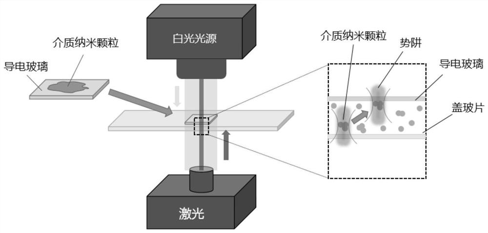
[0044] This example introduces the specific process of preparatory work for the assembly of particles using the optical tweezers system, including the following:
[0045] 1. Put the transparent substrate to be used into acetone, absolute ethanol and deionized water in sequence, and use an ultrasonic oscillator to vibrate and clean for 15 minutes respectively; take out the cleaned transparent substrate, blow off the excess water on the surface with an ear blower and remove it. Dry it on a heating plate, cut the transparent substrate into small pieces of suitable size, and store them separately in the sample box;
[0046] The upper and lower edges of the transparent substrate can also be glued with double-sided adhesive tape of the same thickness. This operation can form a layer of gap between the conductive glass and the cover glass, so that the medium nanoparticle suspension dropped into it has a larger operating space under the optical tweezers, thus facilitating the manipula...
Embodiment 2
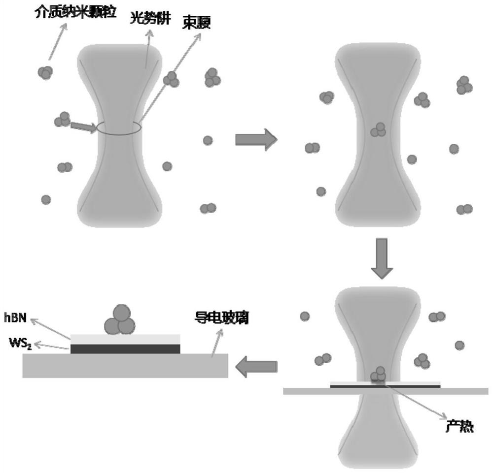
[0051] In this embodiment, the high-refractive medium nanoparticles are fixed on the substrate by creating a potential well to capture the medium nanoparticles and using the photothermal effect. image 3 A schematic diagram of the assembly and immobilization of media nanoparticles is shown, which specifically includes the following steps:
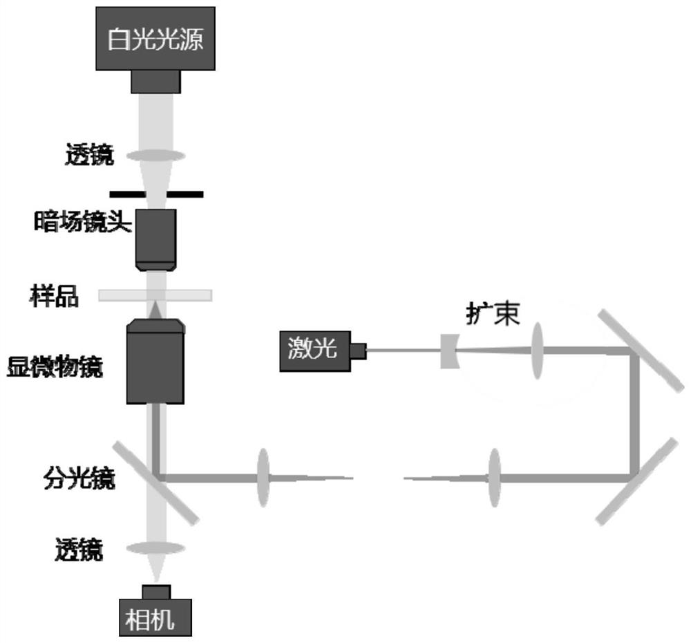
[0052] (1) Turn on the illumination source to the appropriate brightness, coarsely adjust the focus to see if the sample to be processed can be seen through the eyepiece, and fine-tune the focus after seeing the sample to be processed to position the image seen on the substrate surface, and then adjust the sample stage through the joystick Find the position and structure of the particles that need to be assembled in the XY direction. Turn on the computer software of the optical tweezers system to present the imaging picture on the computer screen, adjust the camera frame number and exposure time to make the imaging effect the best, and fine...
Embodiment 3
[0059] In this embodiment, the dark field scattering spectrum of Si nanoparticles fixed on the substrate nanostructure is measured by a single particle dark field spectrum testing system, and the Si nanometers of different sizes and structures are simulated by FDTD (Finite Difference Time Domain). The scattering spectrum of the particles reproduces the experimental spectrum, their optical modes are analyzed, and the structure and size of the Si nanoparticle clusters in the measured medium are determined.
[0060] like Figure 5 Shown is a diagram of the detection device for measuring the dark field scattering spectrum, through which the particles assembled on the nanostructure of the substrate can be measured; first select the Si nanoparticle cluster on the sample, Image 6 1, 2, 3 and 4 all represent Si nanoparticle clusters; then measure the corresponding dark field scattering spectrum by spectrometer, the test results are as follows Figure 7 shown. By analyzing the obtai...
PUM
| Property | Measurement | Unit |
|---|---|---|
| diameter | aaaaa | aaaaa |
Abstract
Description
Claims
Application Information
 - R&D
- Intellectual Property
- Life Sciences
- Materials
- Tech Scout
- Unparalleled Data Quality
- Higher Quality Content
- 60% Fewer Hallucinations
Browse by: Latest US Patents, China's latest patents, Technical Efficacy Thesaurus, Application Domain, Technology Topic, Popular Technical Reports.
© 2025 PatSnap. All rights reserved.Legal|Privacy policy|Modern Slavery Act Transparency Statement|Sitemap|About US| Contact US: help@patsnap.com


