Device and method for performing non-contact photoelectric detection on LED chip

An LED chip, non-contact technology, used in diode testing, single semiconductor device testing, etc., can solve the problems of inability to reflect individual differences, uneven current density, cumbersome testing process, etc., and achieve direct and accurate detection of photoelectric performance. Avoid glowing distracting effects

Active Publication Date: 2021-05-28
XIAMEN UNIV
View PDF18 Cites 3 Cited by
  • Summary
  • Abstract
  • Description
  • Claims
  • Application Information

AI Technical Summary

Problems solved by technology

[0005] However, since LEDs are driven by electricity in practical applications, it is easy to excite non-recombination layer carriers by using light excitation, which is quite different from the electric drive mode and has a high false detection rate.
Moreover, the LED spectrum is measured by photoluminescence. Due to the influence of the excitation light, the spectrometer needs to add a filter, so the test process is cumbersome and the test results are not very accurate.
However, the method of electrically exciting the LED chip by injecting displacement current through the field plate drives all the wafers at one time, and the current density is not uniform, which cannot reflect individual differences.

Method used


Image

  • Device and method for performing non-contact photoelectric detection on LED chip
  • Device and method for performing non-contact photoelectric detection on LED chip
  • Device and method for performing non-contact photoelectric detection on LED chip

Examples


Embodiment 1

[0070] Please refer to figure 1 , Embodiment 1 of the present invention is:

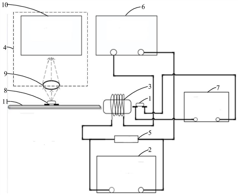
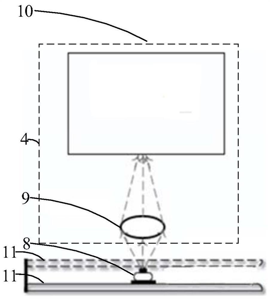
[0071] A device for non-contact photoelectric detection of LED chips, such as figure 1 As shown, it includes a reference LED chip 1 , a shorting device, an oscilloscope 2 , an induction coil 3 , an optical measuring device 4 , a resistor 5 , a first current source 6 and a second current source 7 . Wherein, the oscilloscope 2 is connected in parallel at both ends of the resistor 5, the resistor 5, the first current source 6 and the induction coil 3 are connected in series to form a first closed loop, and the short circuit device is used to place the LED chip 8 to be tested and make the LED chip 8 to be tested The two electrodes are short-circuited to form a second closed loop. The reference LED chip 1 is connected in series with the second current source 7 to form a third closed loop. The second closed loop and the third closed loop are coaxial with the magnetic field direction of the induction coil ...

Embodiment 2

[0073] Please refer to figure 1 and figure 2 , the second embodiment of the present invention is:

[0074] A device for non-contact photoelectric detection of LED chips, on the basis of the first embodiment above, such as figure 1 As shown, the shorting device includes a metal substrate 11, wherein the metal substrate 11 is used to simultaneously contact with the two electrodes of the LED chip 8 to be tested so that the two electrodes of the LED chip 8 to be tested are shorted to form a second closed loop.

[0075] In this example, if figure 2 As shown, the shorting device includes metal substrates 11 located on different sides and electrically connected to each other. Specifically, the metal substrates 11 on different sides are respectively used to contact corresponding electrodes on different sides of the LED chip 8 to be tested so that the two electrodes of the LED chip 8 to be tested are short-circuited to form a second closed loop. figure 2 The structural design sh...

Embodiment 3

[0076] Please refer to image 3 , Embodiment three of the present invention is:

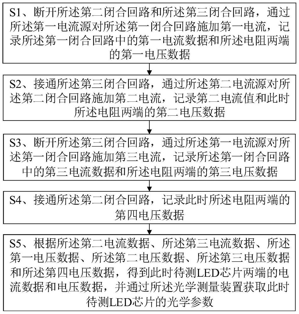
[0077] A method for non-contact photoelectric detection of LED chips, applied to a device for non-contact photoelectric detection of LED chips in Embodiment 1 or Embodiment 2, comprising steps:

[0078] S1, disconnect the second closed loop and the third closed loop, apply the first current to the first closed loop through the first current source 6, record the first current data in the first closed loop and the first voltage data at both ends of the resistor 5 ;

[0079] S2, connect the third closed loop, apply the second current to the second closed loop through the second current source 7, record the second current value and the second voltage data at the two ends of the resistor 5;

[0080] S3. Disconnect the third closed loop, apply a third current to the first closed loop through the first current source 6, and record the third current data in the first closed loop and the third voltage d...


PUM


Abstract

The invention discloses a device and a method for performing non-contact photoelectric detection on an LED chip. The device comprises a reference LED chip, a short circuit device, an oscilloscope, an induction coil, an optical measurement device, a resistor, a first current source and a second current source. The oscilloscope is connected with the two ends of the resistor in parallel, the resistor, the first current source and the induction coil are connected in series to form a first closed loop, the short circuit device is used for placing a to-be-tested LED chip and enabling two electrodes of the to-be-tested LED chip to be in short circuit to form a second closed loop, the reference LED chip and the second current source are connected in series to form a third closed loop, and the second closed loop and the third closed loop are coaxial with the magnetic field direction of the induction coil. The optical measurement device is located on one side of the short circuit device, and the lighting direction is aligned with the to-be-tested LED chip. The device records parameter changes of the circuit in two mutual inductance effect processes, voltage data and current data of the LED chip to be detected are calculated, optical parameters of the LED chip to be detected are obtained, and non-contact photoelectric detection of the LED chip is achieved.

Description

technical field [0001] The invention relates to the technical field of motor control, in particular to a device and method for non-contact photoelectric detection of LED chips. Background technique [0002] LED (Light Emitting Diode) is a semiconductor light-emitting element that can convert electrical energy into light energy. It has the characteristics of high luminous efficiency, small size, long life, fast response, good monochromaticity, power saving and environmental protection, etc. The fourth-generation light sources after incandescent lamps, fluorescent lamps and high-intensity gas discharge lamps are widely used in signal lights, landscape lighting, display technology and other fields. In recent years, they have become a research hotspot in the field of lighting and display. and business attention. [0003] The current detection technology for LED chips is mainly divided into two directions: contact type and non-contact type. The basic core content of the contact...

Claims


Application Information

Patent Timeline
IPC IPC(8): G01R31/26
CPCG01R31/2635
Inventor 吕毅军张人予倪祖荣钟晨明朱丽虹高玉琳陈忠
Owner XIAMEN UNIV
Why Eureka
Try Eureka