A liquid crystal writing device and method for realizing partial erasing by using light
A writing device and partial technology, applied in optics, nonlinear optics, data processing input/output process, etc., can solve the problems of increasing design complexity and production cost, unable to realize partial erasing, affecting display effect, etc., to achieve Improve the control accuracy and partial erasing accuracy, reduce the complexity of the circuit structure, and the effect of simple circuit structure
- Summary
- Abstract
- Description
- Claims
- Application Information
AI Technical Summary
Problems solved by technology
Method used
Image

Examples
Embodiment 1
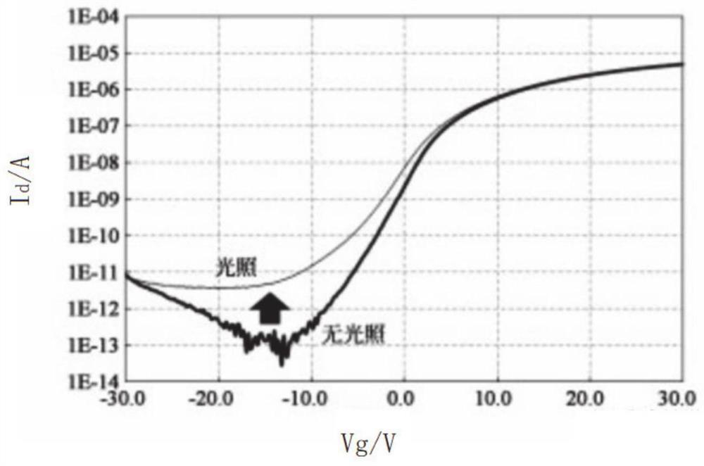
[0046] As described in the background technology, the influence of light on the conduction characteristics of TFTs will affect the normal display of liquid crystal displays. Therefore, measures need to be taken to overcome this influence in the prior art, and it is not thought of to make full use of it to solve liquid crystal writing. Partial erasure of the device.
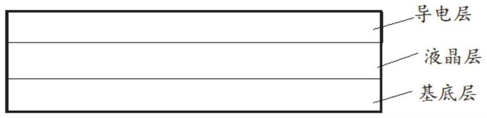
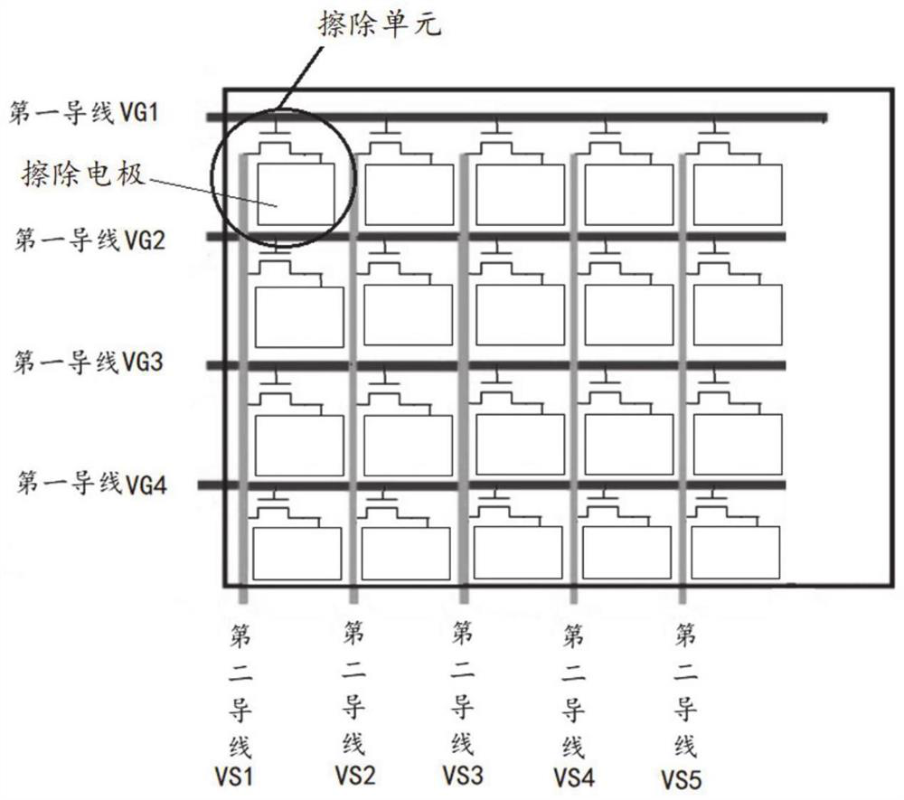
[0047] According to an embodiment of the present invention, an embodiment of a liquid crystal writing device that utilizes light to realize partial erasing is disclosed. Refer to figure 2 and image 3 , including: a conductive layer, a bistable liquid crystal layer and a base layer arranged sequentially from top to bottom. Wherein, the conductive layer may not be divided, and several erasing units are integrated on the base layer, and these erasing units are arranged in an array, and each erasing unit is provided with an erasing electrode and a TFT connected to the erasing electrode; The conduction can provide ...
Embodiment 2
[0070] According to an embodiment of the present invention, an embodiment of an optical erasing device is disclosed. The optical erasing device can be applied to the liquid crystal writing device that utilizes light to realize partial erasing in Embodiment 1, so as to provide a setting intensity. Illumination to achieve local erasure.
[0071] In this embodiment, the optical erasing device provides illumination with a set intensity; the optical erasing device includes: a power supply unit, an illumination unit, an infrared detection unit, a state detection unit and a trigger unit;
[0072] Wherein, the power supply unit provides power supply for other units; the lighting unit is used to provide a light source with a set light intensity.
[0073] The state detection unit is used to detect the space pose state of the erasing piece, and when it detects that the optical erasing device is in the set space pose state, send a trigger signal to the trigger unit.
[0074] The infrared...
Embodiment 3
[0083] According to an embodiment of the present invention, an embodiment of a method for partially erasing a liquid crystal writing device is disclosed. The method is based on the structure of a liquid crystal writing device that uses light to achieve partial erasing disclosed in Embodiment 1. The implementation process is as follows:
[0084] Applying a set voltage to the conductive layer, applying a set control voltage and an input voltage to the TFTs in all or set part of the erasing unit of the base layer, so that the TFTs are in a critical cut-off state; wherein, the control voltage is for the gate The voltage provided by the pole, and the input voltage is the voltage applied to the source.
[0085] Applying light with a set intensity to the area to be erased can turn on the TFT of the erasing unit in the corresponding area, thereby applying a set second voltage to the corresponding erasing electrode, and applying a third voltage to the conductive layer. The second voltage ...
PUM
 Abstract
Description
Claims
Application Information
 - R&D
- Intellectual Property
- Life Sciences
- Materials
- Tech Scout
- Unparalleled Data Quality
- Higher Quality Content
- 60% Fewer Hallucinations
Browse by: Latest US Patents, China's latest patents, Technical Efficacy Thesaurus, Application Domain, Technology Topic, Popular Technical Reports.
© 2025 PatSnap. All rights reserved.Legal|Privacy policy|Modern Slavery Act Transparency Statement|Sitemap|About US| Contact US: help@patsnap.com