Efficient passivation structure battery and preparation method thereof
A battery and high-efficiency technology, applied in the field of solar cells, can solve the problems of efficiency failure, compactness, and poor thickness uniformity, and achieve the effects of improving efficiency, reducing contact resistance, and improving uniformity
- Summary
- Abstract
- Description
- Claims
- Application Information
AI Technical Summary
Problems solved by technology
Method used
Image
Examples
preparation example Construction
[0038] A kind of preparation method of described efficient passivation structure battery, comprises following preparation steps:
[0039] 1) Obtain P-type crystalline silicon and make texture, the resistivity of P-type crystalline silicon is 0.5-1.5Ω·cm;
[0040] 2) Diffusion, laser SE and etching of the P-type crystalline silicon after texturing to obtain a semi-finished product with a clean surface;
[0041] 3) After etching, the semi-finished product is prepared by oxidation method for double-sided silicon dioxide;
[0042] 4), double-sided silicon dioxide wafer source for backside Ga 2 o 3 / AlN / Ta 2 o 5 Preparation of laminated passivation film, the thickness of which is 2-15nm;
[0043] 5) Continue to deposit silicon oxynitride + silicon nitride composite laminated film on the back, wherein silicon nitride is on the top layer;
[0044] 6) Deposit silicon nitride + silicon oxynitride composite laminate film on the front side, in which silicon oxynitride is on the top...
Embodiment 1
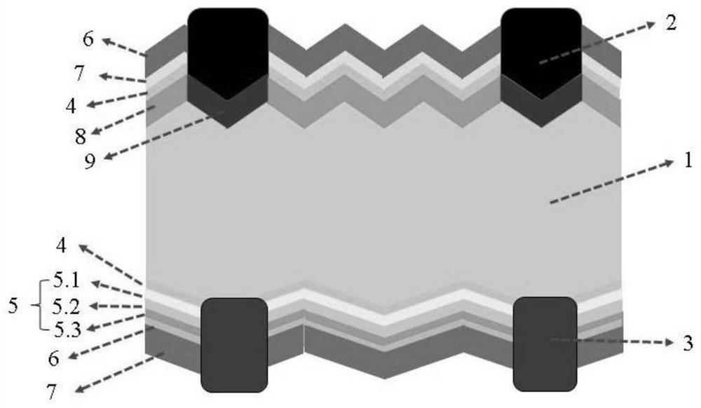
[0048] A high-efficiency passivation structure battery, comprising a P-type crystalline silicon 1, two negative electrodes 2 arranged on the front of the P-type crystalline silicon 1, and two positive electrodes 3 arranged on the back of the P-type crystalline silicon 1, the The back side of the P-type crystalline silicon 1 is provided with SiO 2 Layer 4, the SiO 2 Layer 4 is provided with Ga 2 o 3 / AlN / Ta 2 o 5 A passivation film 5 is laminated. The front side of the P-type crystalline silicon 1 is sequentially provided with an N+ layer 8, SiO 2 Layer 4, SiN x Layer 7 and SiO x N y layer 6, the negative electrode 2 goes through the SiO x N y Layer 6, SiN x Layer 7, SiO 2 Layer 4 and N+ layer 8. The contact area between the negative electrode 2 and the P-type crystalline silicon 1 is provided with an N++ layer 9 . The back side of the P-type crystalline silicon 1 is sequentially provided with SiO 2 Layer 4, Ga 2 o 3 / AlN / Ta 2 o 5 Laminated passivation film 5...
Embodiment 2
[0059] A high-efficiency passivation structure battery, comprising a P-type crystalline silicon 1, two negative electrodes 2 arranged on the front of the P-type crystalline silicon 1, and two positive electrodes 3 arranged on the back of the P-type crystalline silicon 1, the The back side of the P-type crystalline silicon 1 is provided with SiO 2 Layer 4, the SiO 2 Layer 4 is provided with Ga 2 o 3 / AlN / Ta 2 o 5 A passivation film 5 is laminated. The front side of the P-type crystalline silicon 1 is sequentially provided with an N+ layer 8, SiO 2 Layer 4, SiN x Layer 7 and SiO x N y layer 6, the negative electrode 2 goes through the SiO x N y Layer 6, SiN x Layer 7, SiO 2Layer 4 and N+ layer 8. The contact area between the negative electrode 2 and the P-type crystalline silicon 1 is provided with an N++ layer 9 . The back side of the P-type crystalline silicon 1 is sequentially provided with SiO 2 Layer 4, Ga 2 o 3 / AlN / Ta 2 o 5 Laminated passivation film 5,...
PUM
| Property | Measurement | Unit |
|---|---|---|
| Thickness | aaaaa | aaaaa |
| Resistivity | aaaaa | aaaaa |
| Resistivity | aaaaa | aaaaa |
Abstract
Description
Claims
Application Information
 - R&D
- Intellectual Property
- Life Sciences
- Materials
- Tech Scout
- Unparalleled Data Quality
- Higher Quality Content
- 60% Fewer Hallucinations
Browse by: Latest US Patents, China's latest patents, Technical Efficacy Thesaurus, Application Domain, Technology Topic, Popular Technical Reports.
© 2025 PatSnap. All rights reserved.Legal|Privacy policy|Modern Slavery Act Transparency Statement|Sitemap|About US| Contact US: help@patsnap.com


