Method for simultaneously preparing, packaging and using multiple chips

A chip and chip array technology, which is applied in the field of simultaneous preparation and packaging of multiple chips, can solve the problems of increased cost of SiC material devices, achieve increased process complexity, low design complexity and manufacturing process complexity, and enhance product application value Effect

Active Publication Date: 2021-03-26
NO 55 INST CHINA ELECTRONIC SCI & TECHNOLOGYGROUP CO LTD
View PDF4 Cites 0 Cited by
  • Summary
  • Abstract
  • Description
  • Claims
  • Application Information

AI Technical Summary

Problems solved by technology

However, the extremely small size will also increase the cost of SiC material devices, mainly including the complexity of chip dicing and the complexity of chip extraction, etc.

Method used


Image

  • Method for simultaneously preparing, packaging and using multiple chips
  • Method for simultaneously preparing, packaging and using multiple chips
  • Method for simultaneously preparing, packaging and using multiple chips

Examples


Embodiment

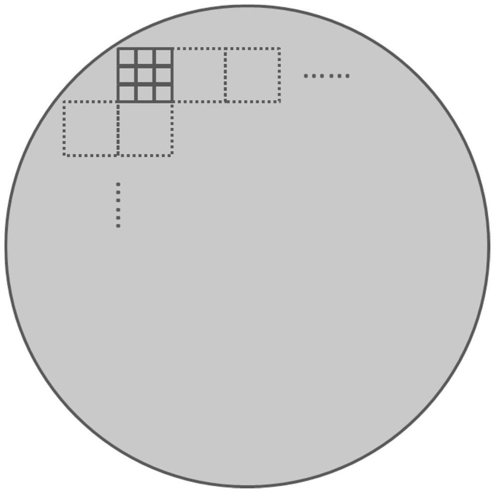
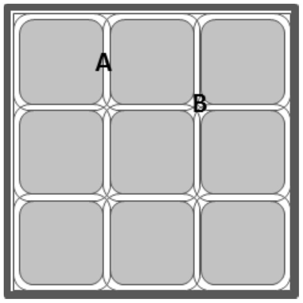
[0036] The invention discloses a method for preparing, packaging and using multiple chips at the same time. It is mainly suitable for small-volume, high-power silicon carbide devices. The application situation is mainly for array units. This invention is mainly but not limited to the following: Condition:

[0037] When used in module A, if multiple same low-current chips are required, the chips in the array can be used in different positions of the module through an external circuit;

[0038] B In circuits that require high reliability, since the chips in the array unit are taped out of the same batch and the same chip, the device consistency is high, and the devices can back up each other;

[0039] C Even only from the perspective of cost reduction, the different chips of the array unit are connected in parallel and independent of each other. Through testing and screening, waste chips in the array unit can be eliminated without wire bonding (or not used in the circuit after w...


PUM


Abstract

The invention discloses a method for simultaneously preparing, packaging and using multiple chips. The method comprises the following step of: optimizing layout design of a wafer where a device chip is located; optimizing the specific structural design of the device chip; keeping an original micromachining process flow and difficulty unchanged; and simplifying a device scribing and packaging use process, and reducing the total preparation cost of the device. According to the method, through design optimization, the workload of the device in test, scribing and chip picking stages is reduced, and the purposes of reducing the cost and improving the product competitiveness are achieved; and especially, the method has good potential application value for silicon carbide-based devices and otherdevices with small sizes and high power.

Description

technical field [0001] The invention relates to the field of semiconductor devices, in particular to a method for preparing and packaging multiple chips at the same time. Background technique [0002] SiC materials have large bandgap width, high breakdown electric field, high saturation drift velocity and high thermal conductivity. The superior properties of these materials make them ideal materials for making high-power, high-frequency, high-temperature-resistant, and radiation-resistant devices. Therefore, SiC materials can often achieve the same electrical performance as other semiconductor materials (especially silicon) with a smaller volume. However, the extremely small size will also increase the cost of SiC material devices, mainly including the complexity of chip dicing and chip extraction. [0003] The advantage of silicon carbide in particular lies in the fabrication of high-voltage devices. For high-voltage device chips, a terminal structure with a certain width...

Claims


Application Information

Patent Timeline
IPC IPC(8): H01L25/00H01L21/56H01L25/07H01L29/06
CPCH01L25/50H01L21/561H01L25/07H01L29/0623H01L29/0615H01L29/0684
Inventor 陈允峰李士颜刘昊陈谷然黄润华柏松
Owner NO 55 INST CHINA ELECTRONIC SCI & TECHNOLOGYGROUP CO LTD
Why Eureka
Try Eureka