Semiconductor structure and forming method thereof

A semiconductor, multi-layer structure technology, applied in semiconductor/solid-state device manufacturing, electrical components, circuits, etc., can solve the problem that the accuracy of pattern transfer needs to be improved

Pending Publication Date: 2021-03-23
SEMICON MFG INT (SHANGHAI) CORP +1
View PDF0 Cites 0 Cited by
  • Summary
  • Abstract
  • Description
  • Claims
  • Application Information

AI Technical Summary

Problems solved by technology

[0003] However, in the process of forming semiconductor structures in the prior art, the accuracy of pattern transfer needs to be improved

Method used


Image

  • Semiconductor structure and forming method thereof
  • Semiconductor structure and forming method thereof
  • Semiconductor structure and forming method thereof

Examples


Embodiment Construction

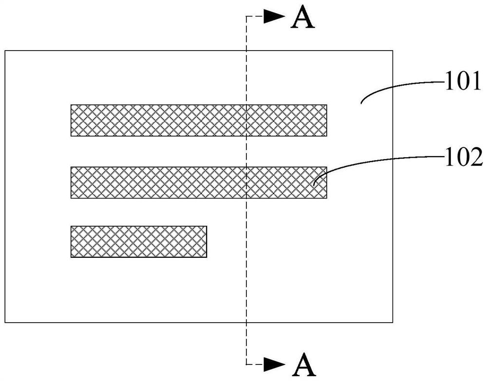
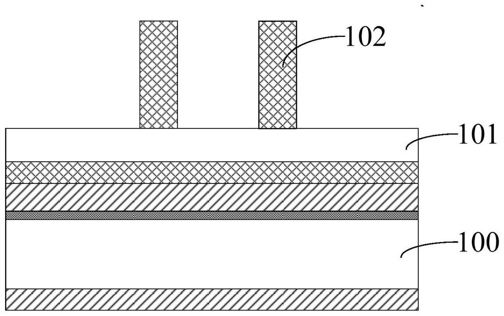
[0031] As mentioned in the background art, in the process of forming a semiconductor structure in the prior art, the accuracy of pattern transfer needs to be improved. The following will combine Figure 1 to Figure 4 Be explained, Figure 1 to Figure 4 It is a structural schematic diagram of each step in the formation process of a semiconductor structure.

[0032] Please refer to figure 1 and figure 2 , figure 2 Yes figure 1 A schematic cross-sectional view along line A-A, providing a layer to be etched 100; forming an initial mask layer 101 on the layer to be etched 100; forming an exposed portion of the initial mask layer 101 on the initial mask layer 101 Graphical structure 102 of .

[0033] Please refer to image 3 and Figure 4 , Figure 4 Yes image 3 A schematic cross-sectional view along line A-A, using the patterned structure 102 as a mask, ion doping treatment is performed on the initial mask layer 101 to form a mask layer (not shown), and the mask layer ...


PUM

PropertyMeasurementUnit
heightaaaaaaaaaa
thicknessaaaaaaaaaa

Abstract

The invention discloses a semiconductor structure and a forming method thereof. The forming method comprises the steps of providing a to-be-etched layer; forming an initial mask layer on the to-be-etched layer; forming a graphical structure exposing a part of the initial mask layer on the initial mask layer; forming a barrier layer on the surface of the side wall of the graphical structure; takingthe graphical structure and the barrier layer as masks, carrying out ion doping processing on the initial mask layer, and forming a doped region and an undoped region in the initial mask layer; and removing the graphical structure and the barrier layer; after removing the graphical structure and the barrier layer, removing the undoped region, forming a mask layer on the surface of the to-be-etched layer , forming a first opening exposing the top surface of the to-be-etched layer in the mask layer. The barrier layer is formed on the surface of the side wall of the graphical structure, so thatdoped ions can be effectively prevented from entering the graphical structure to enter the undoped region, so that the undoped region will not be decreased; since the consistency of the undoped regionand the graphical structure is effectively improved by using the barrier layer, and the accuracy of pattern transfer is improved.

Description

technical field [0001] The invention relates to the technical field of semiconductor manufacturing, in particular to a semiconductor structure and a forming method thereof. Background technique [0002] In the semiconductor integrated circuit manufacturing process, a semiconductor structure is formed on a semiconductor substrate through a series of procedures, such as deposition, photolithography, etching, and the like. Among them, the photolithography process is to form a desired pattern in the photoresist, obtain a patterned photoresist, and define a region to be etched. The etching process is used to transfer the pattern in the patterned photoresist to the layer to be etched. [0003] However, in the process of forming semiconductor structures in the prior art, the accuracy of pattern transfer needs to be improved. Contents of the invention [0004] The technical problem solved by the present invention is to provide a semiconductor structure and its forming method, wh...

Claims


Application Information

Patent Timeline
Patent Type & Authority Applications(China)
IPC IPC(8): H01L21/306H01L21/308H01L21/027
CPCH01L21/30604H01L21/308H01L21/0274H01L21/0332H01L21/0335H01L21/0337H01L21/0338
Inventor 张前江苏波窦涛孙林林
Owner SEMICON MFG INT (SHANGHAI) CORP
Why Eureka
Try Eureka