


Quick Research
Generate reliable direction feasibility study reports for your R&D in just a few steps.

Technical Q&A
Discover and master advanced knowledge NOW. Basics, ideas, possibilities, all at once.

Find Solutions
As an expert in R&D theories, this can generate solutions to your technical problems instantly.

Evaluate Feasibility
Analyze your overall solution with one click, know your potential R&D risks in advance.

Monitor Landscape
Get weekly tech updates, stay abreast of the latest tech innovations and key insights.
3D printing device and method for repairing faults of circuit board
A 3D printing and 3D printer technology, applied in the field of 3D printing, can solve the problems of high difficulty and low efficiency when repairing circuit boards
- Summary
- Abstract
- Description
- Claims
- Application Information
AI Technical Summary
Problems solved by technology
Method used
Image

Examples
Embodiment 1
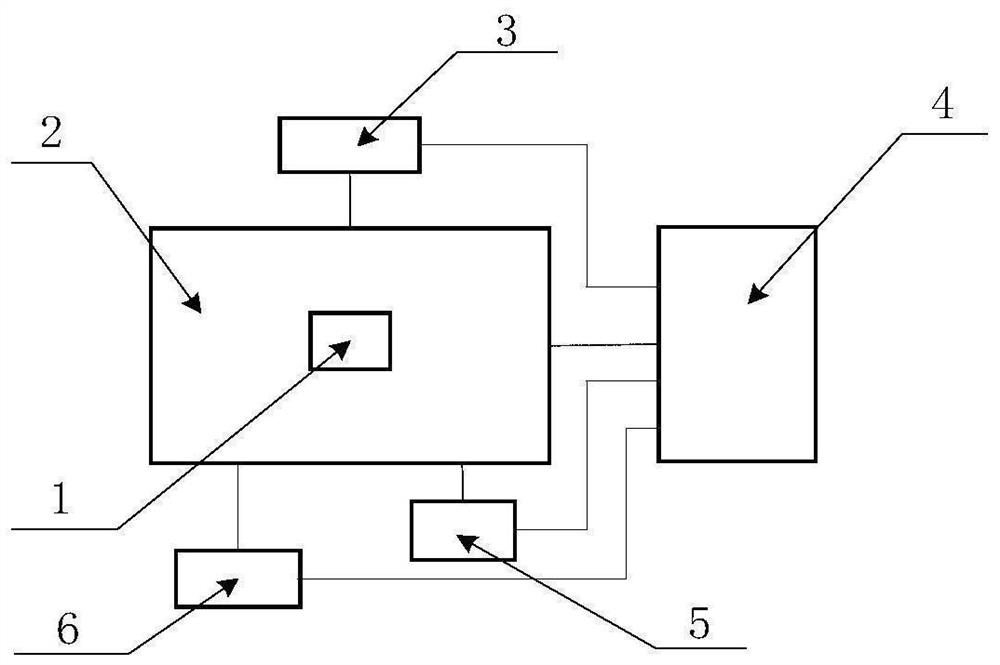
[0019] A kind of 3D printing device that is used to repair circuit board failure, comprises micro-jet 3D printer 2, and described micro-jet 3D printer 2 is installed with industrial camera 3, four-probe measuring instrument 6 above its workbench, industrial camera 3 and The micro-jet 3D printer 2 is electrically connected to the controller 4 through wires; the micro-jet 3D printer 2 is provided with an infrared laser 5 that moves with the printer nozzle on the working arm where the printer nozzle is installed; wherein the controller 4 Realize the control of the working path of the infrared laser 5 by controlling the working arm of the micro-jet 3D printer 2 while realizing the micro-jet 3D printer 2 injection path and the injection volume; the controller 4 is also used to receive pictures taken by the industrial camera 3 information and carry out the identification of the photographed content in order to detect the fault area; the industrial camera 3 is used to photograph the c...
Embodiment 2
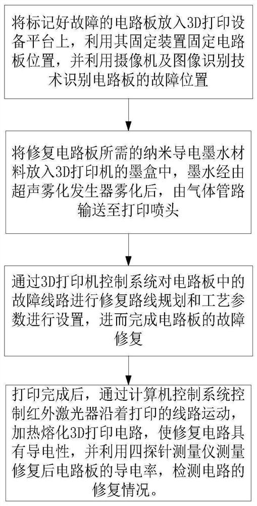
[0021] A method for utilizing the 3D printing device described in embodiment 1 for repairing circuit board faults, wherein the method comprises the following steps: 1), the circuit board 1 marking the fault position is placed on the work of the micro-jet 3D printer 2 on the platform, and use the fixing device on the working platform to fix the circuit board 1, the controller 4 takes pictures of the circuit board 1 through the industrial camera 3, and uses image recognition technology to identify the fault location of the circuit board 1;
[0022] 2) Put the nano-conductive ink material required for repairing the circuit board 1 into the ink cartridge of the micro-jet 3D printer 2. After the nano-conductive ink material is atomized by the ultrasonic atomization generator, it is transported to the micro-jet 3D printer by the gas pipeline 2 print heads;
[0023] 3), carry out the planning of repairing circuit to the circuit fault in circuit board 1 by controller 4, and set proces...
PUM
 Abstract
Description
Claims
Application Information
 - R&D Engineer
- R&D Manager
- IP Professional
- Industry Leading Data Capabilities
- Powerful AI technology
- Patent DNA Extraction
Browse by: Latest US Patents, China's latest patents, Technical Efficacy Thesaurus, Application Domain, Technology Topic, Popular Technical Reports.
© 2024 PatSnap. All rights reserved.Legal|Privacy policy|Modern Slavery Act Transparency Statement|Sitemap|About US| Contact US: help@patsnap.com