Wafer processing device and wafer processing method

A processing device and processing method technology, applied in electrical components, semiconductor/solid-state device manufacturing, circuits, etc., can solve the problem of large total thickness deviation, low etching rate of wafer center, and low utilization rate of chemical liquid in wet cleaning equipment, etc. question

Pending Publication Date: 2021-03-16
UNITED MICROELECTRONICS CENT CO LTD
View PDF4 Cites 0 Cited by
  • Summary
  • Abstract
  • Description
  • Claims
  • Application Information

AI Technical Summary

Problems solved by technology

[0003] The technical problem to be solved by the present invention is to provide a wafer processing device and a wafer processing method to solve the problems of low utilization rate of chemical solution in wet cleaning equipment, low etching rate at the center of the wafer, and total thickness deviation after wet etching Large, poor consistency, and difficult adjustments

Method used


Image

  • Wafer processing device and wafer processing method
  • Wafer processing device and wafer processing method

Examples


Embodiment Construction

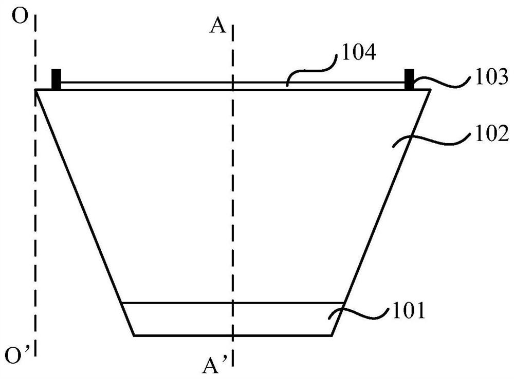
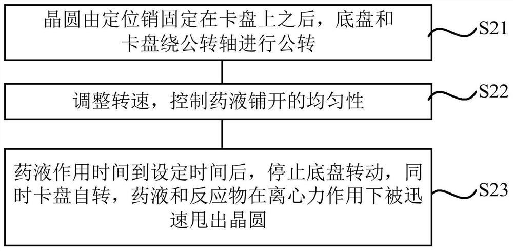
[0009] Specific implementations of a wafer processing device and a wafer processing method provided by the present invention will be described in detail below with reference to the accompanying drawings.

[0010] attached figure 1 Shown is a schematic structural diagram of the wafer processing device described in a specific embodiment of the present invention, including:

[0011] Wafer carrier, used to carry the wafer 104; a revolution drive device, the revolution drive device can drive the wafer carrier to rotate along a revolution axis OO', the revolution axis OO' is located outside the wafer carrier; A driving device, the rotation driving device can drive the wafer carrier to rotate along a rotation axis AA', the rotation axis AA' is located at the center of the wafer carrier and perpendicular to the surface of the wafer 104 .

[0012] The wafer carrier includes: a chuck 102, the chuck 102 is used to place the wafer 104, and can rotate; the chassis 101, the chassis 101 is ...


PUM


Abstract

The invention relates to a wafer processing device and a wafer processing method. The device comprises a wafer carrier which is used for bearing a wafer; a revolution driving device which can drive the wafer carrier to rotate along a revolution shaft, wherein the revolution shaft is located outside the wafer carrier; and an autorotation driving device which can drive the wafer carrier to rotate along an autorotation shaft, wherein the autorotation shaft is located at the circle center of the wafer carrier and is perpendicular to the surface of the wafer. The wafer processing method comprises acleaning step and a liquid medicine throwing step, wherein in the cleaning step, a wafer is driven to rotate along a revolution shaft by adopting a revolution driving device; in the liquid medicine throwing step, an autorotation driving device is adopted to drive the wafer to rotate along an autorotation shaft. The invention aims to etch the wafer by designing the wafer processing device into a mode of combining revolution and rotation, optimize the total thickness deviation and consistency of the wafer, control the etching rate of the wafer, improve the utilization rate of liquid medicine tothe maximum extent and reduce the manufacturing cost.

Description

technical field [0001] The invention relates to the field of semiconductor equipment, in particular to a wafer processing device and a wafer processing method. Background technique [0002] In the prior art, wafer processing devices generally use a device in which the wafer is fixed on the chuck by positioning pins, and the wafer rotates with the chuck. After the chemical liquid of this device is sprayed out, under the action of centrifugal force, it is thrown from the center of the wafer to the edge of the wafer. This leads to low etching rate at the center of the wafer, large deviation and poor consistency of the total thickness after wet etching, and also problems such as difficult adjustment and low utilization rate of the chemical solution. Contents of the invention [0003] The technical problem to be solved by the present invention is to provide a wafer processing device and a wafer processing method to solve the problems of low utilization rate of chemical solutio...

Claims


Application Information

Patent Timeline
Patent Type & Authority Applications(China)
IPC IPC(8): H01L21/687H01L21/67
CPCH01L21/68792H01L21/6708H01L21/67253
Inventor 吕相林
Owner UNITED MICROELECTRONICS CENT CO LTD
Why Eureka
Try Eureka