Semiconductor structure and forming method thereof

A technology of semiconductor and isolation structure, applied in the field of semiconductor structure and its formation, can solve the problem that the performance of semiconductor structure needs to be improved, and achieve the effect of improving performance and avoiding short circuit

Pending Publication Date: 2021-05-07
SEMICON MFG INT (SHANGHAI) CORP +1
View PDF0 Cites 0 Cited by
  • Summary
  • Abstract
  • Description
  • Claims
  • Application Information

AI Technical Summary

Problems solved by technology

[0003] However, as the size of transistors becomes smaller, the performance of the formed semiconductor structures has yet to be improved

Method used


Image

  • Semiconductor structure and forming method thereof
  • Semiconductor structure and forming method thereof
  • Semiconductor structure and forming method thereof

Examples


Embodiment Construction

[0027] As mentioned in the background, the performance of existing semiconductor structures still needs to be improved. Now analyze and illustrate in conjunction with specific embodiment.

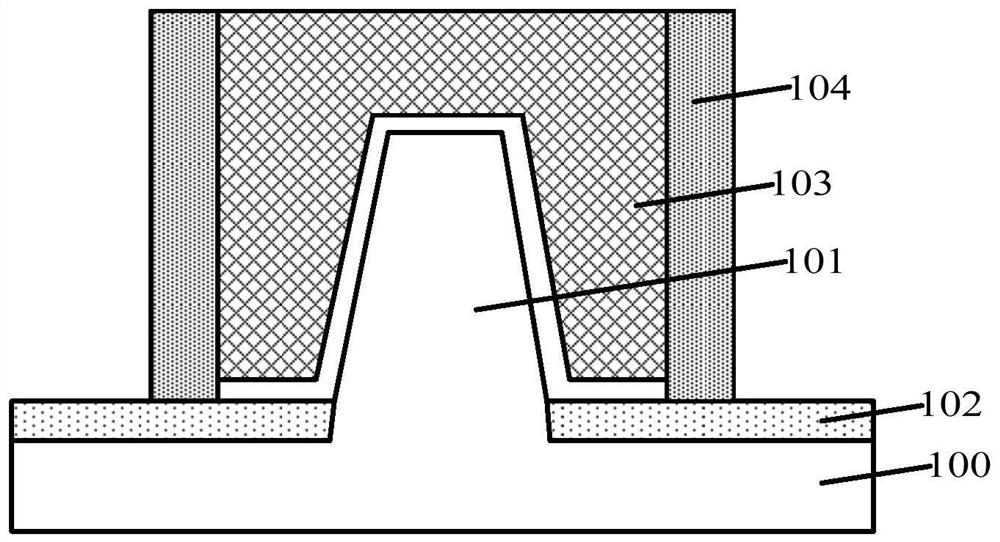
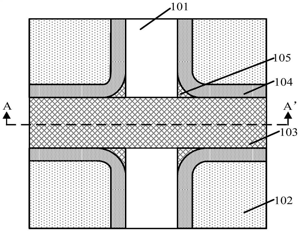
[0028] figure 1 and figure 2 It is a schematic cross-sectional structure diagram of a semiconductor structure in an embodiment.

[0029] Please refer to figure 1 and figure 2 , figure 1 for figure 2 Schematic diagram along section line AA', figure 2 for figure 1 The top view of the structure includes: a substrate 100 with a fin 101 on the substrate 100; an isolation structure 102 located on the substrate and part of the sidewall of the fin 101; a dummy gate structure 103 located on the substrate 100, the dummy The gate structure 103 spans the fin portion 101 ; the sidewall 104 is located on the sidewall of the dummy gate structure 103 .

[0030] In the semiconductor structure, when forming the dummy gate structure 103, it is necessary to form a dummy gate material layer (not sh...


PUM


Abstract

The invention discloses a semiconductor structure and a forming method thereof. The method comprises the steps that a substrate which is provided with a fin structure is provided; a dummy gate layer crossing the fin structure is formed on the substrate, the dummy gate layer comprises a main body part and an extension part, the main body part crosses part of the side wall surface and part of the top surface of the fin structure, the top of the extension part is lower than the top surface of the fin structure, and the extension part is located at a corner formed by part of the side wall of the fin structure and the side wall of the main body part; and the extension part is removed by adopting a first cleaning process. The performance of the semiconductor structure formed by the method is improved.

Description

technical field [0001] The invention relates to the field of semiconductor manufacturing, in particular to a semiconductor structure and a forming method thereof. Background technique [0002] With the rapid development of semiconductor manufacturing technology, semiconductor devices are developing towards higher element density and higher integration. Transistors, as the most basic semiconductor devices, are currently being widely used. Therefore, as the component density and integration of semiconductor devices increase, the size of transistors is also getting smaller and smaller. [0003] However, as the size of transistors gets smaller, the performance of the resulting semiconductor structures has yet to be improved. Contents of the invention [0004] The technical problem solved by the present invention is to provide a semiconductor structure and its forming method, so as to improve the performance of the semiconductor structure. [0005] In order to solve the above...

Claims


Application Information

Patent Timeline
IPC IPC(8): H01L21/336H01L29/78H01L21/3213
CPCH01L29/66795H01L29/66545H01L29/785H01L21/32134
Inventor 张静刘佳磊
Owner SEMICON MFG INT (SHANGHAI) CORP
Why Eureka
Try Eureka