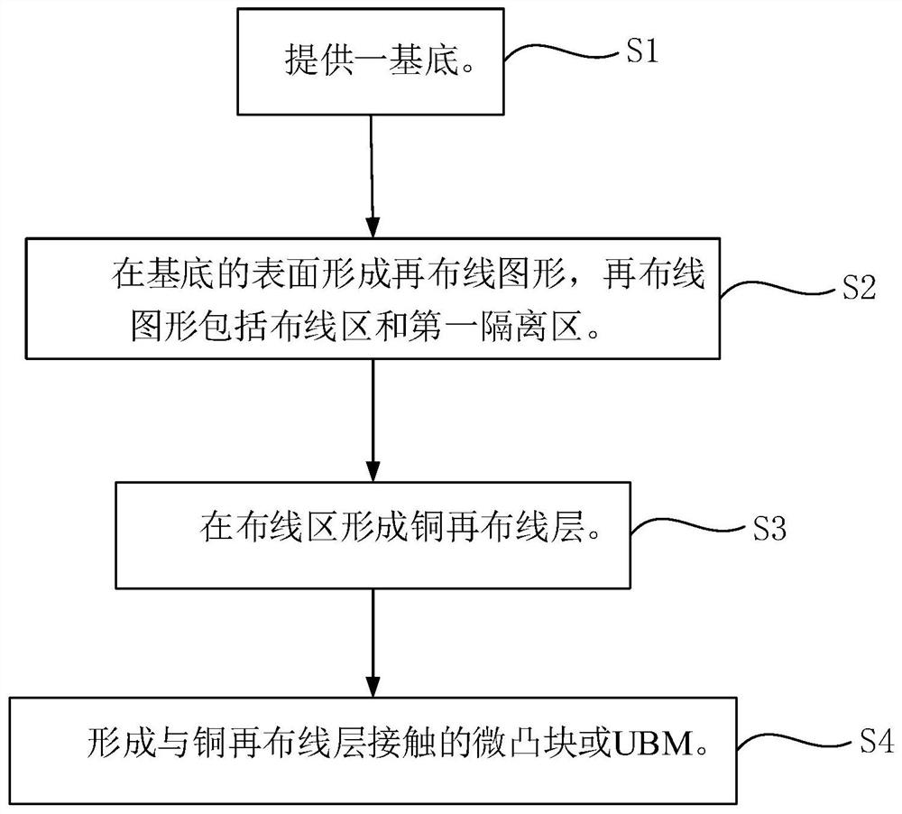
Manufacturing method of copper rewiring layer, silicon optical device and chip
A technology of rewiring layer and manufacturing method, which is applied in the manufacturing of semiconductor devices, electric solid-state devices, semiconductor/solid-state devices, etc., can solve the problems of low conductivity, large skin effect, insufficient high-frequency characteristics, etc., and achieve high electrical performance. , Good high frequency characteristics, small skin effect
- Summary
- Abstract
- Description
- Claims
- Application Information
AI Technical Summary
Problems solved by technology
Method used
Image


Examples
Embodiment Construction
[0030] In order to clearly describe the technical solutions of the embodiments of the present invention, in the embodiments of the present invention, words such as "first" and "second" are used to distinguish the same or similar items with basically the same function and effect. For example, the first threshold and the second threshold are only used to distinguish different thresholds, and their sequence is not limited. Those skilled in the art can understand that words such as "first" and "second" do not limit the number and execution order, and words such as "first" and "second" do not necessarily limit the difference.
[0031] It should be noted that, in the present invention, words such as "exemplary" or "for example" are used as examples, illustrations or illustrations. Any embodiment or design described herein as "exemplary" or "for example" should not be construed as being preferred or advantageous over other embodiments or designs. Rather, the use of words such as "ex...
PUM
 Abstract
Description
Claims
Application Information
 - R&D
- Intellectual Property
- Life Sciences
- Materials
- Tech Scout
- Unparalleled Data Quality
- Higher Quality Content
- 60% Fewer Hallucinations
Browse by: Latest US Patents, China's latest patents, Technical Efficacy Thesaurus, Application Domain, Technology Topic, Popular Technical Reports.
© 2025 PatSnap. All rights reserved.Legal|Privacy policy|Modern Slavery Act Transparency Statement|Sitemap|About US| Contact US: help@patsnap.com