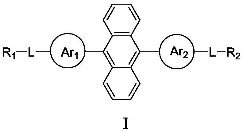
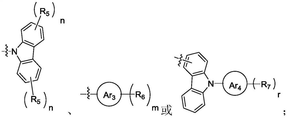
Anthracene compound and organic light emitting diode device
A compound and anthracene-based technology, applied in the field of organic electroluminescence, can solve problems such as uncertain molecular weight, poor batch stability, and affecting device performance, and achieve the goals of definite structure and molecular weight, good batch stability, and reduced production costs Effect
- Summary
- Abstract
- Description
- Claims
- Application Information
AI Technical Summary
Problems solved by technology
Method used
Image
Examples
preparation example Construction
[0122]Preparation method of organic light emitting diode device:
[0123](1) First, clean the ITO substrate in the following order: 5% KOH solution ultrasonic for 15 minutes, pure water ultrasonic for 15 minutes, isopropanol ultrasonic for 15 minutes, and oven drying for 1 hour; then the substrate is transferred to UV-OZONE equipment for surface treatment for 15 minutes. Transfer to the glove box immediately after finishing.
[0124](2) Spin-coating a layer of hole injection layer material, namely PEDOT:PSS film, on a clean ITO substrate, and then bake it at 230°C for 15 minutes. A layer of HTL film, namely VNPB, is spin-coated on the hole injection layer, and the film is baked at 200°C for 30 minutes after the film is spin-coated.
[0125](3) A layer of HTL film, namely VNPB, is spin-coated on the hole injection layer, and the film is baked at 200°C for 30 minutes after being spin-coated into a film.
[0126](4) Dissolve the anthracene compound with the solvent o-xylene and prepare a solution,...
Embodiment 1
[0129]Using compound M1 as the light-emitting layer material, the organic light-emitting diode device 1 is prepared according to the structure and preparation method of the above-mentioned organic light-emitting diode device.
Embodiment 2~6
[0131]Using the compounds M2 to M6 as the light-emitting layer material (M), according to the structure and preparation method of the above-mentioned organic light-emitting diode device, the organic light-emitting diode devices 2-6 are respectively prepared.
PUM
| Property | Measurement | Unit |
|---|---|---|
| thickness | aaaaa | aaaaa |
Abstract
Description
Claims
Application Information
 - R&D
- Intellectual Property
- Life Sciences
- Materials
- Tech Scout
- Unparalleled Data Quality
- Higher Quality Content
- 60% Fewer Hallucinations
Browse by: Latest US Patents, China's latest patents, Technical Efficacy Thesaurus, Application Domain, Technology Topic, Popular Technical Reports.
© 2025 PatSnap. All rights reserved.Legal|Privacy policy|Modern Slavery Act Transparency Statement|Sitemap|About US| Contact US: help@patsnap.com


