A volatile and nonvolatile cuxo memristor and its control method

A non-volatile, memristor technology, applied in electrical components and other directions, can solve problems such as unfavorable cost control, little mention of memristor volatility, complex process, etc. The effect of improved cell life and number of operations, and high mobility

Active Publication Date: 2022-08-05
HUAZHONG UNIV OF SCI & TECH
View PDF6 Cites 0 Cited by
  • Summary
  • Abstract
  • Description
  • Claims
  • Application Information

AI Technical Summary

Problems solved by technology

In some literatures, it is also mentioned to dope the active metal in the functional layer to achieve the volatile and non-volatile transition of the device, but the doping process may introduce impurity ions, and the process is complicated, which is not conducive to cost control
In addition, many literatures have studied Cu-based 2 Non-volatility of memristors with O functional layer, but with respect to Cu 2 Volatility of O memristors rarely mentioned

Method used


Image

  • A volatile and nonvolatile cuxo memristor and its control method
  • A volatile and nonvolatile cuxo memristor and its control method
  • A volatile and nonvolatile cuxo memristor and its control method

Examples


Embodiment 1

[0038] Example 1: A kind of Cu with both volatile and non-volatile x O memristor preparation method

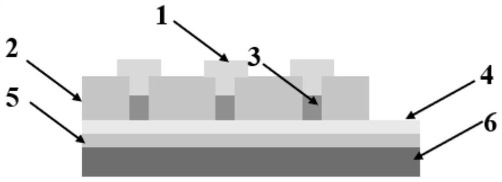
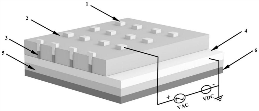
[0039] The Cu provided in this example x O memristor, TiN / Cu with pinhole structure x O / Pt memristor, whose structure is as figure 1 and figure 2 shown; in which the lower electrode is Pt with a thickness of 100 nm; the functional layer Cu x The thickness of O is 60 nm; the insulating layer on the lower electrode is SiO 2 , the total thickness is 100nm; the upper electrode is TiN, the thickness is 100nm.

[0040] The Cu will be specifically explained below x The preparation method of O memristor:

[0041] (1) Preparation of lower electrode

[0042] Substrate cleaning: Si / SiO 2 The substrate was immersed in analytically pure acetone for experimental use, placed in an ultrasonic cleaner with a power of 60w, and sonicated for 10 minutes; the samples cleaned with acetone were immersed in analytically pure ethanol for experimental use, and ultrasonicated for 10 minutes; t...

Embodiment 2

[0056] Example 2: A TiN / Cu with both volatile and non-volatile x O / Pt memristor control method

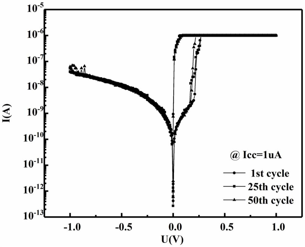
[0057] In the regulation and test stage, the test adopts DC test. Generally speaking, it can be carried out according to the following steps:

[0058] (1) Forming is performed on the selected memristor unit, and the first electrical operation causes Cu vacancies to start to migrate and redistribute, forming an unstable conductive channel; wherein the limiting current in the Forming process is selected as 50uA, and the voltage sweep range is 0V-5V;

[0059] (2) The memristor unit is set to limit the current and tested.

[0060] The following is the Cu prepared in Example 1 x The method for regulating and testing the memristor specifically includes the following steps:

[0061] (1) Select a memristor unit on the sample, tie the two probes to the upper electrode and the reserved lower electrode area respectively, apply a positive voltage to the probe connected to the upper electro...


PUM

PropertyMeasurementUnit
thicknessaaaaaaaaaa
thicknessaaaaaaaaaa
thicknessaaaaaaaaaa

Abstract

The invention belongs to the technical field of microelectronic devices, and discloses a Cu having both volatile and non-volatile properties x O memristor and control method thereof, comprising a bottom electrode layer (4), a functional layer (3) and an upper electrode layer (1) stacked from bottom to top, wherein the functional layer (3) is Cu x O functional layer, x satisfies 1.8<x<2, the functional layer is deposited in the insulating layer, specifically by etching through holes in the insulating layer, and then depositing the functional layer to make the functional layer contact the lower electrode layer; the upper electrode layer is deposited on top of the functional layer. The present invention improves the key structure and composition of the memristor, and uses Cu x O is the functional layer, 1.8<x<2, the stoichiometry is close to Cu 2 O, can obtain both volatile and nonvolatile Cu x O memristor, the Cu x O memristors are based on Cu vacancy modulation, which can be volatile and nonvolatile by simply confining current to induce Cu vacancies to construct synapses and conductive filaments.

Description

technical field [0001] The invention belongs to the technical field of microelectronic devices, and more particularly, relates to a kind of Cu having both volatile and non-volatile properties x O memristor and its control method, the memristor can induce Cu vacancies to form clusters and conductive filaments by limiting current, realize the transition between volatile and non-volatile devices, and can be used for neuromorphic computing and artificial synapse realization. Background technique [0002] Volatile threshold transition (TS) and nonvolatile resistive switching (MS) are two typical responses of memristors to voltage. Nonvolatile resistive switching behavior can be applied in scenarios such as data storage and synaptic simulation. Loss of threshold transition behavior is used in circuit switches and analog neurons due to its nonlinear resistance change; in the current research hot artificial neural network construction, both volatile and non-volatile memristors are r...

Claims


Application Information

Patent Timeline
Patent Type & Authority Patents(China)
IPC IPC(8): H01L45/00
CPCH10N70/801H10N70/821H10N70/20H10N70/8833H10N70/011
Inventor 孙华军王涛缪向水
Owner HUAZHONG UNIV OF SCI & TECH
Why Eureka
Try Eureka