Manufacturing method of embedded circuit board, embedded circuit board and application

A manufacturing method and circuit board technology, which is applied in printed circuit manufacturing, multilayer circuit manufacturing, and chemical/electrolytic methods to remove conductive materials, etc., can solve the problem of high heat generation, high resistance of aluminum-copper alloys, and failure to meet user product performance Requirements and other issues to achieve a good heat dissipation effect

Pending Publication Date: 2021-01-08
SHENNAN CIRCUITS
View PDF5 Cites 0 Cited by
  • Summary
  • Abstract
  • Description
  • Claims
  • Application Information

AI Technical Summary

Problems solved by technology

[0003] However, in the long-term research and development process, the inventor of the present application found that when welding the aluminum foil pad and the copper circuit layer, it is easy to obtain an aluminum-copper alloy, and the aluminum-copper alloy has a large resistance, which will cause high energy consumption and high heat generation of the circuit board. , which seriously affects the stability of circuit board products, and cannot meet the different product performance requirements of users.

Method used


Image

  • Manufacturing method of embedded circuit board, embedded circuit board and application
  • Manufacturing method of embedded circuit board, embedded circuit board and application
  • Manufacturing method of embedded circuit board, embedded circuit board and application

Examples


Embodiment Construction

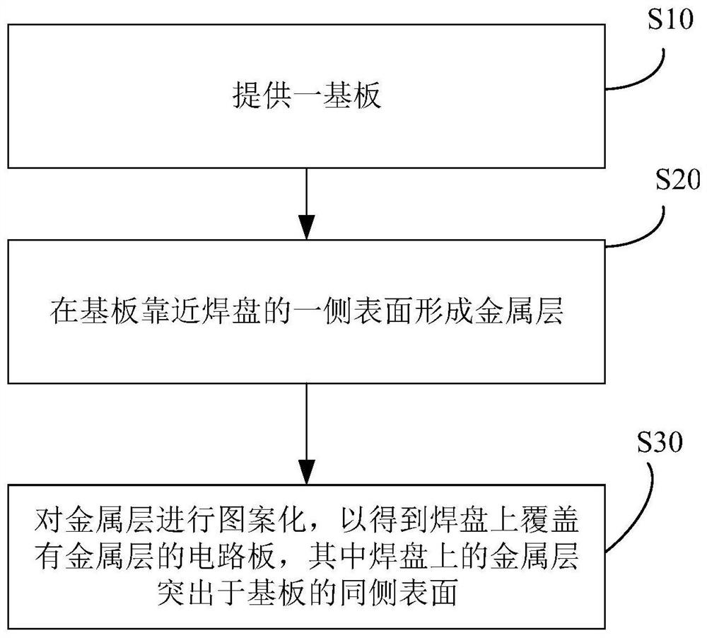
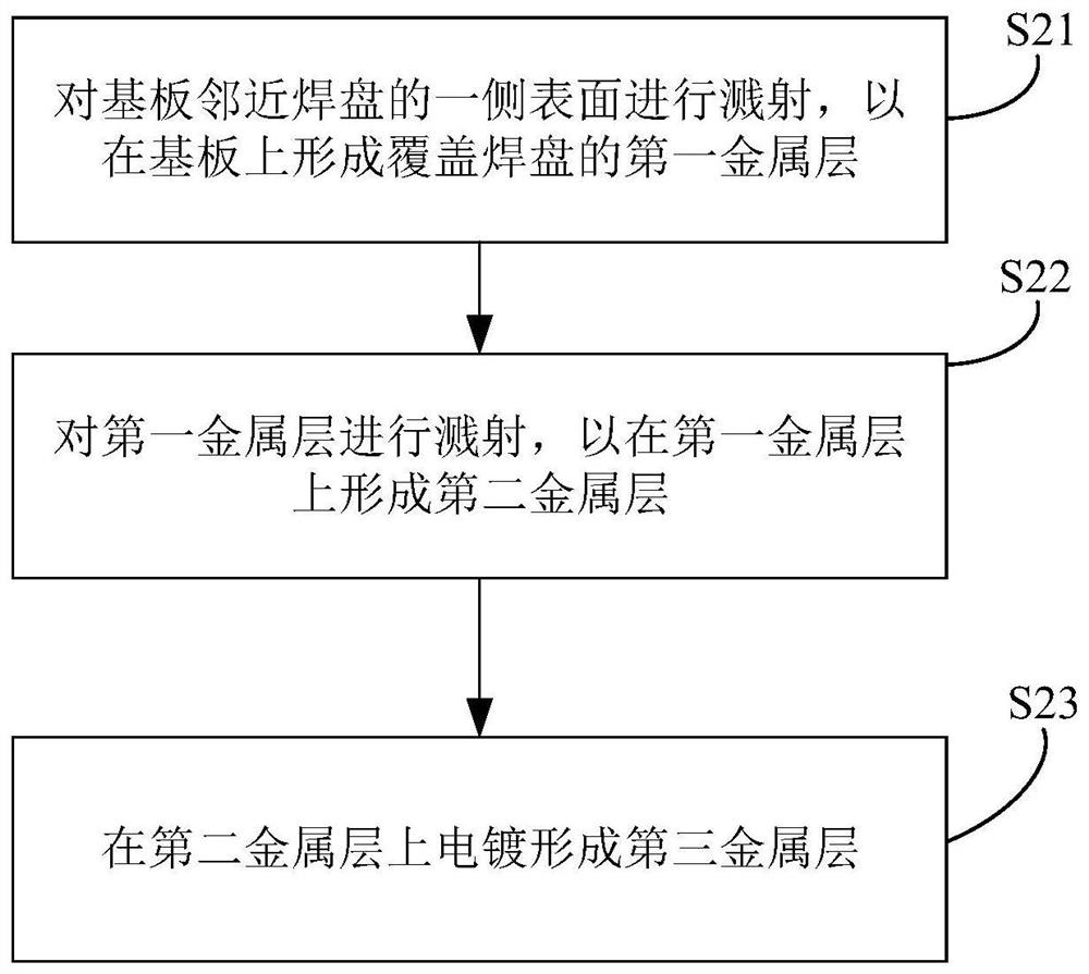
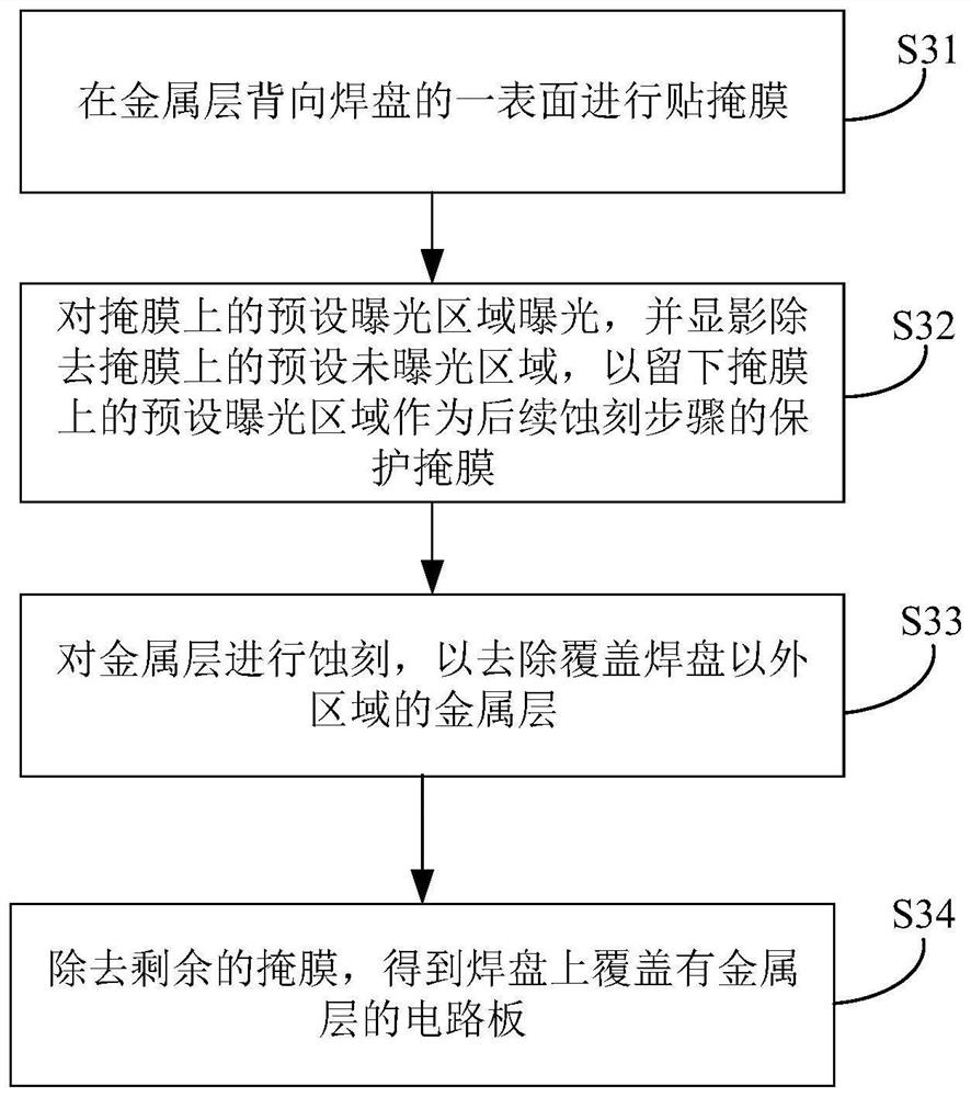
[0021] The following will clearly and completely describe the technical solutions in the embodiments of the present application with reference to the drawings in the embodiments of the present application. Obviously, the described embodiments are only some of the embodiments of the present application, not all of them. Based on the embodiments in this application, all other embodiments obtained by persons of ordinary skill in the art without making creative efforts belong to the scope of protection of this application.

[0022] All directional indications (such as up, down, left, right, front, back...) in the embodiments of the present application are only used to explain the relative positional relationship between the various components in a certain posture (as shown in the drawings) , sports conditions, etc., if the specific posture changes, the directional indication also changes accordingly. Furthermore, the terms "include" and "have", as well as any variations thereof, a...


PUM


Abstract

The invention relates to the technical field of circuit boards, and particularly discloses a manufacturing method of an embedded circuit board, the embedded circuit board and application, the method comprises the following steps: providing a substrate, embedding an electronic device in the substrate, arranging a bonding pad on the surface of one side of the electronic device, and flushing the endsurface of the bonding pad with the surface of the same side of the substrate; forming a metal layer on the surface of one side, close to the bonding pad, of the substrate; and patterning the metal layer to obtain the circuit board with the bonding pad covered with the metal layer, the metal layer on the bonding pad protruding out of the surface of the same side of the substrate. By means of the above manner, secondary processing can be conducted on the bonding pads on the substrate according to user requirements, and then the embedded circuit board meeting different product performance requirements of users is manufactured.

Description

technical field [0001] The present application relates to the technical field of circuit boards, in particular to a method for manufacturing an embedded circuit board, the embedded circuit board and its application. Background technique [0002] As we all know, the metals with the best electrical conductivity are silver, copper, gold, and aluminum. In the electronics industry, especially in the circuit board industry, among the above metals with the best electrical conductivity, gold and silver, which are expensive, are rarely used in the circuit board industry. Existing semiconductor manufacturers usually use aluminum foil as the base material for electronic devices. The pad material is used to quickly dissipate the heat generated when the electronic device is working, and the copper foil is used as the copper circuit layer material. [0003] However, in the long-term research and development process, the inventor of the present application found that when welding the alum...

Claims


Application Information

Patent Timeline
Patent Type & Authority Applications(China)
IPC IPC(8): H05K3/22H05K3/40H05K1/11H05K1/09H05K1/18
CPCH05K1/185H05K1/0271H05K1/0298H05K3/32H05K2201/0195H05K1/18H05K3/00H01L23/498H01L21/48H01L21/56H01L25/16H01L23/31H05K1/02H05K3/46H05K1/11H05K3/42H05K3/30H05K3/28H05K1/03H01L25/00H05K3/22H05K3/40H05K1/09H01L23/142H01L23/49822H01L23/49827H01L23/5389H05K1/188H05K3/06H05K3/4602H05K2201/0317H05K2201/0338H05K1/165H05K2201/086H05K3/188H05K2203/0723H05K2201/09063H05K2201/09072H05K1/111H05K1/115H05K1/183H05K3/061H05K3/143H05K3/146H05K3/16H05K3/4038H05K2201/0183H01F27/06H01F27/24H01F27/324H01F41/127H01F2027/065
Inventor 黄立湘王泽东缪桦
Owner SHENNAN CIRCUITS
Why Eureka
Try Eureka