


Quick Research
Generate reliable direction feasibility study reports for your R&D in just a few steps.

Technical Q&A
Discover and master advanced knowledge NOW. Basics, ideas, possibilities, all at once.

Find Solutions
As an expert in R&D theories, this can generate solutions to your technical problems instantly.

Evaluate Feasibility
Analyze your overall solution with one click, know your potential R&D risks in advance.

Monitor Landscape
Get weekly tech updates, stay abreast of the latest tech innovations and key insights.
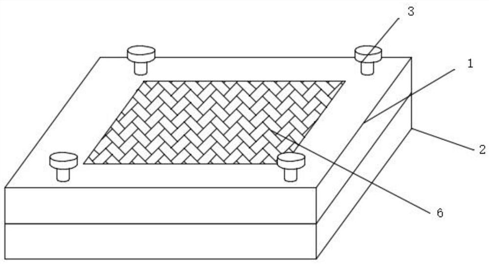
Bonding pad through hole packaging equipment for processing image sensing chip
A technology for sensing chips and packaging equipment, applied in radiation control devices, electrical components, electrical solid devices, etc. Good stability, good encapsulation state, and the effect of ensuring stability
- Summary
- Abstract
- Description
- Claims
- Application Information
AI Technical Summary
Problems solved by technology
Method used
Image

Examples
Embodiment approach
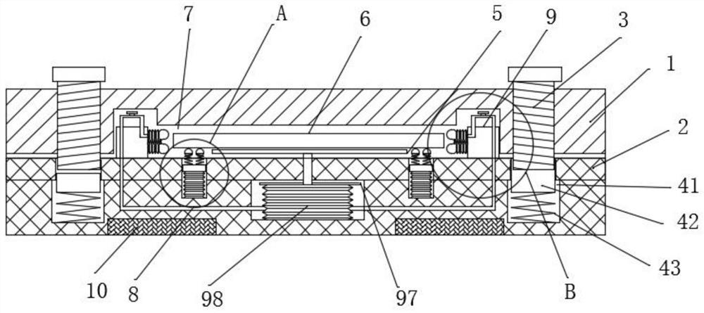
[0026] As an embodiment of the present invention, the positioning assembly 9 includes a positioning bar 91, a shut-off valve 92, a contraction spring 93, a limit bar 94, a contraction plate 95, a limit air bag 96, an extrusion plate 97 and an air storage bag 98, packaged The central position of the bottom plate 2 is provided with a storage tank, and the air storage bag 98 is arranged in the storage tank, and the positioning bars 91 are erected on the top side of the package base plate 2 respectively, and the space-limiting air bags 96 are respectively installed on the opposite surfaces of the two positioning bars 91 to limit A contraction plate 95 is pasted on the end inwall of the position air bag 96, and a contraction spring 93 is affixed between the contraction plate 95 and the sidewall of the positioning bar 91, and two limit strips 94 are pasted on the end face of the space limit air bag 96.
[0027] As an embodiment of the present invention, an extruding plate 97 is fixed...
PUM
 Abstract
Description
Claims
Application Information
 - R&D Engineer
- R&D Manager
- IP Professional
- Industry Leading Data Capabilities
- Powerful AI technology
- Patent DNA Extraction
Browse by: Latest US Patents, China's latest patents, Technical Efficacy Thesaurus, Application Domain, Technology Topic, Popular Technical Reports.
© 2024 PatSnap. All rights reserved.Legal|Privacy policy|Modern Slavery Act Transparency Statement|Sitemap|About US| Contact US: help@patsnap.com