Gallium oxide-based heterojunction integrated photoelectric chip, remote ultraviolet array monitor and manufacturing method of remote ultraviolet array monitor

A gallium oxide-based, optoelectronic chip technology, applied in photometry, measurement of ultraviolet rays, circuits, etc. using electric radiation detectors, can solve the attenuation of sterilization effects, affect the application effect, and it is difficult to detect the intensity of ultraviolet radiation and the range of wavelengths, etc. question

Active Publication Date: 2020-12-04
杭州紫芯光电有限公司
View PDF7 Cites 1 Cited by
  • Summary
  • Abstract
  • Description
  • Claims
  • Application Information

AI Technical Summary

Problems solved by technology

[0003] Although the existing ultraviolet light is widely used, the disadvantage of ultraviolet light is that the longer it is used, the weaker the radiation intensity will be, and the bactericidal effect will continue to decay.
It is difficult to detect whether the radiation intensity and band range of ultraviolet rays are qualified, which will affect the application effect, and the existing ultraviolet detectors are usually measured for a certain band, so it is impossible to directly judge whether the ultraviolet band meets the requirements for use

Method used


Image

  • Gallium oxide-based heterojunction integrated photoelectric chip, remote ultraviolet array monitor and manufacturing method of remote ultraviolet array monitor
  • Gallium oxide-based heterojunction integrated photoelectric chip, remote ultraviolet array monitor and manufacturing method of remote ultraviolet array monitor
  • Gallium oxide-based heterojunction integrated photoelectric chip, remote ultraviolet array monitor and manufacturing method of remote ultraviolet array monitor

Examples


Embodiment 1

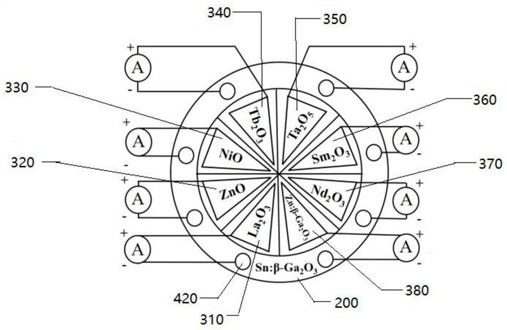
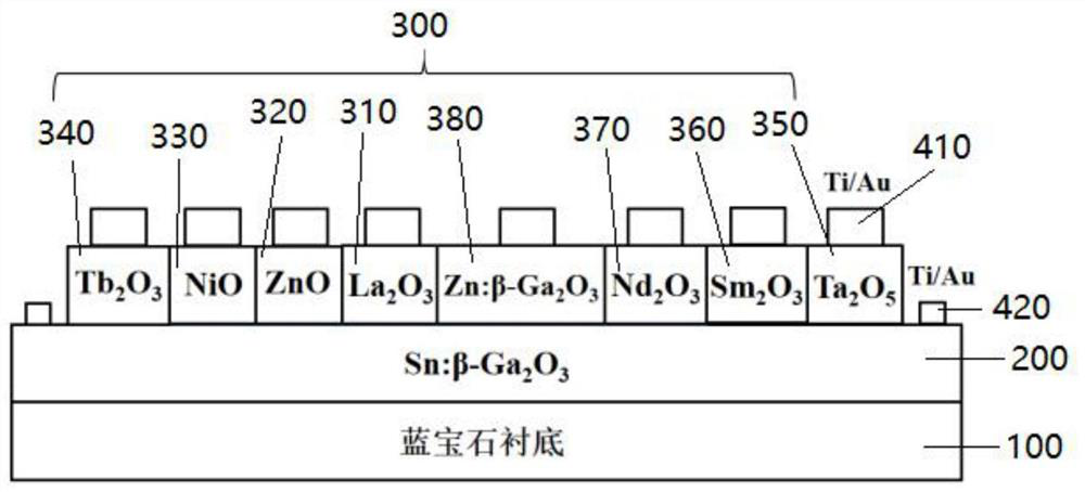
[0035] like Figure 1-2 As shown, a wide-ranging gallium oxide-based heterojunction integrated optoelectronic chip includes a sapphire single crystal substrate 100, Sn:β-Ga 2 o 3 Circular film 200 and composite film 300; Wherein said composite film 300 comprises La located on the same plane and arranged in a circle 2 o 3 Thin film 310, ZnO thin film 320, NiO thin film 330, Tb 2 o 3 Film 340, Ta 2 o 5 Film 350, Sm 2 o 3 Film 360, Nd 2 o 3 Thin film 370 and Zn:β-Ga 2 o 3 Thin film 380, adopted in Sn:β-Ga 2 o 3 A composite film composed of a plurality of films is formed on the circular film 200, which can form a La 2 o 3 / Sn:β-Ga 2 o 3 、ZnO / Sn:β-Ga 2 o 3 、NiO / Sn:β-Ga 2 o 3 , Tb 2 o 3 / Sn:β-Ga 2 o 3 、 Ta 2 o 5 / Sn:β-Ga 2 o 3 、Sm 2 o 3 / Sn:β-Ga 2 o 3 、Nd 2 o 3 / Sn:β-Ga 2 o 3 and Zn:β-Ga 2 o 3 / Sn:β-Ga 2 o 3 Heterojunction structure, in which ZnO, NiO, Tb 2 o 3 、 Ta 2 o 5 、Sm 2 o 3 , Nd 2 o 3 、Zn:β-Ga 2 o 3 and La 2 o 3 The forbid...

Embodiment 2

[0039] A method for manufacturing a UV-C / B / A remote ultraviolet array monitor with continuously adjustable wavelength has the following steps:

[0040] (1) Preparation of gallium oxide-based heterojunction integrated optoelectronic chips:

[0041] Put the c-plane sapphire circular single crystal substrate into V(HF):V(H 2 o 2 )=1:5 solution soaked to remove the natural oxide layer, then ultrasonically cleaned with acetone, ethanol and deionized water, and vacuum-dried; the 99.99% pure Ga 2 o 3 , La 2 o 3 , ZnO, NiO, Tb 2 o 3 、 Ta 2 o 5 、Sm 2 o 3 and Nd 2 o 3 The targets are respectively placed on the target stage of the multi-target laser pulse deposition system. 2 o 3 Place a Sn metal ring around the glow circle of the target, fix the c-plane sapphire circular single crystal substrate after the above treatment on the sample holder, put it into the vacuum chamber, each target and the c-plane sapphire circular single crystal substrate The distance between them is...

Embodiment 3

[0058] Step (2) is identical with embodiment 2. In step (1), put the c-plane sapphire circular single crystal substrate into V(HF):V(H 2 o 2 )=1:5 solution soaked to remove the natural oxide layer, then ultrasonically cleaned with acetone, ethanol and deionized water, and vacuum-dried; the 99.99% pure Ga 2 o 3 , La 2 o 3 , ZnO, NiO, Tb 2 o 3 、 Ta 2 o 5 、Sm 2 o 3 and Nd 2 o 3 The targets are respectively placed on the target stage of the multi-target laser pulse deposition system. 2 o 3 Place a Sn metal ring around the glow circle of the target, fix the above-mentioned c-plane sapphire circular single crystal substrate on the sample holder, put it into the vacuum chamber, each target and the c-plane sapphire circular single crystal substrate The distance between them is 5 cm; the cavity is evacuated first, argon gas is introduced, the pressure in the vacuum cavity is adjusted, the sapphire single crystal substrate is heated, and the Sn-doped Ga 2 o 3 thin film, ...


PUM

PropertyMeasurementUnit
thicknessaaaaaaaaaa
thicknessaaaaaaaaaa
thicknessaaaaaaaaaa

Abstract

The invention relates to a gallium oxide-based heterojunction integrated photoelectric chip, a remote ultraviolet array monitor and a manufacturing method of the remote ultraviolet array monitor. Thegallium oxide-based heterojunction integrated photoelectric chip comprises a sapphire single crystal substrate, a Sn:beta-Ga2O3 circular film and a composite film which are sequentially arranged, wherein the composite film comprises a La2O3 film, a ZnO film, a NiO film, a Tb2O3 film, a Ta2O5 film, a Sm2O3 film, an Nd2O3 film and a Zn:beta-Ga2O3 film which are located on the same plane and arrangedinto a circle, and further comprises an upper Ti/Au film electrode and a lower Ti/Au film electrode which are in one-to-one correspondence, the upper Ti/Au film electrode is formed on the composite film and is in one-to-one correspondence with the La2O3 film, the ZnO film, the NiO film, the Tb2O3 film, the Ta2O5 film, the Sm2O3 film, the Nd2O3 film and the Zn:beta-Ga2O3 film, and the lower Ti/Aufilm electrode is located on the Sn:beta-Ga2O3 circular film. The gallium oxide-based heterojunction integrated chip prepared by the invention is stable in performance, has high responsivity and sensitivity to a broadband ultraviolet spectrum, is low in dark current, can intelligently identify the wavelength of ultraviolet rays, and has a great application prospect.

Description

technical field [0001] The invention belongs to the technical field of ultraviolet monitoring devices, and in particular relates to a gallium oxide-based heterojunction integrated photoelectric chip, a UV-C / B / A remote ultraviolet array monitor with continuously adjustable wavelength and a preparation method thereof. Background technique [0002] Common ultraviolet wave bands are between 200nm-380nm, and different wave bands have different functions and can be used in different application fields, among which UVA (320nm-380nm) is used in the field of ultraviolet curing; UVB (280 nm-320nm) is used in ultraviolet health care; UVC (200nm-280nm) has a strong bactericidal effect, and is mainly used in hospitals, disease control centers, kindergartens, canteens and other places that require ultraviolet sterilization. [0003] Although the existing ultraviolet light is widely used, the disadvantage of ultraviolet light is that the longer it is used, the weaker the radiation intensit...

Claims


Application Information

Patent Timeline
Patent Type & Authority Applications(China)
IPC IPC(8): H01L31/0336H01L31/109H01L31/18G01J1/44
CPCH01L31/109H01L31/0336H01L31/18G01J1/429G01J1/44Y02P70/50
Inventor 王顺利郭道友
Owner 杭州紫芯光电有限公司
Why Eureka
Try Eureka