Infrared detector splicing module and infrared detector integrated assembly
A technology of infrared detectors and module substrates, applied in the field of infrared detectors, can solve the problems of inability to realize splicing of super large area array infrared detectors, no consideration of electrical integration, poor scalability, etc., and achieve good temperature uniformity and scope of application Wide range of effects with high module reliability
- Summary
- Abstract
- Description
- Claims
- Application Information
AI Technical Summary
Problems solved by technology
Method used
Image

Examples
Embodiment 1
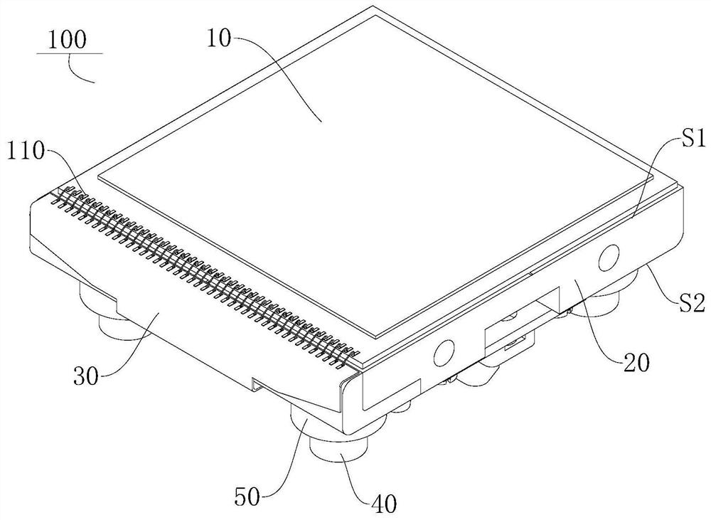
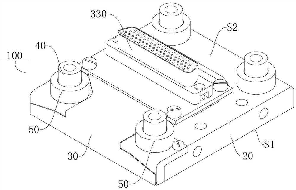
[0080] Such as Figure 1-Figure 9 As shown, in this embodiment, the infrared detector splicing module 100 includes: an infrared detector chip 10 , a module substrate 20 , an electrical module 30 , a support column 40 and a leveling gasket 50 .
[0081] Wherein, the module substrate 20 is made of SiC material. combine figure 1 with Figure 5 As shown, the infrared detector chip 10 is glued onto the first surface S1 of the module substrate 20 by low temperature adhesive. The side surface of the module substrate 20 reserves a threaded hole h3 for connection with the splicing tooling. At the same time, if Figure 5 with Image 6 As shown, around the first surface S1 bonded with the infrared detector chip 10, high-precision photolithography marks 201 are processed for chip bonding and positioning.
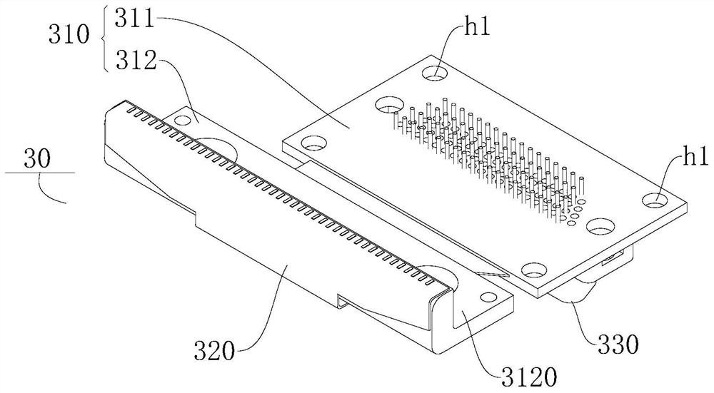
[0082] Such as image 3 with Figure 4 As shown, the electrical module 30 includes: a fixing board 310 , a flexible circuit board 320 and an electrical insert 330 .
[0083]Whe...
Embodiment 2
[0096] Such as Figure 10-15 As shown, the difference from Embodiment 1 is that in this embodiment, the infrared detector chip 10 has double terminals 110 , and there are two electrical modules 30 , and the two electrical modules 30 are electrically connected to one of the terminals 110 . That is to say, for the infrared detector chip 10 with double leads 110, two electrical modules 30 can be set, wherein the two electrical modules 30 share a first board body 311 and an electrical plug-in 330, and the two electrical modules 30 of the infrared detector chip 10 Each lead-out terminal 110 is lead out from the electrical plug-in 330 on the second surface S2 of the module substrate 20 through two flexible circuit boards 320 .
[0097] Correspondingly, as Figure 16 with Figure 17 As shown, it is an integrated assembly 1000 formed by splicing a plurality of infrared detector splicing modules 100 with double leads 110 to a splicing substrate 900 .
Embodiment 3
[0099] Such as Figure 18 with Figure 19 As shown, the difference from Embodiment 1 is that in this embodiment, there are three support columns 40, so that when a plurality of splicing modules 100 are spliced and connected, the assembly efficiency can be improved, and the number of splicing modules 100 can be reduced. The Z direction is over-constrained. The Z direction mentioned here can be understood as the axial direction of the support column 40 .
PUM
 Abstract
Description
Claims
Application Information
 - R&D
- Intellectual Property
- Life Sciences
- Materials
- Tech Scout
- Unparalleled Data Quality
- Higher Quality Content
- 60% Fewer Hallucinations
Browse by: Latest US Patents, China's latest patents, Technical Efficacy Thesaurus, Application Domain, Technology Topic, Popular Technical Reports.
© 2025 PatSnap. All rights reserved.Legal|Privacy policy|Modern Slavery Act Transparency Statement|Sitemap|About US| Contact US: help@patsnap.com