Solar cell based on double perovskite material and preparation method of solar cell
A solar cell, double perovskite technology, applied in circuits, photovoltaic power generation, electrical components, etc., can solve the problems of tin-based perovskite instability, poor environment, water stability and air stability, etc. The effect of chemical production, improving photoelectric response and good stability
- Summary
- Abstract
- Description
- Claims
- Application Information
AI Technical Summary
Problems solved by technology
Method used
Image
Examples
Embodiment 1
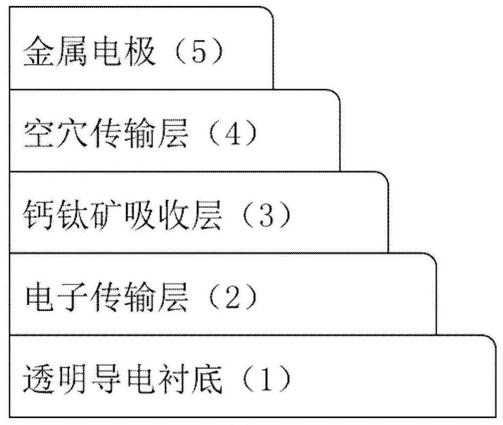
[0033] Example 1: Preparation of transparent conductive substrate using indium tin oxide ITO, electron transport layer using [6,6]-phenyl C 61 Methyl butyrate PCBM, perovskite light absorbing layer using Cs 2 AgInBr 6 , the hole transport layer uses 3,4-ethylenedioxythiophene: polystyrene sulfonate PEDOT:PSS, and the top metal electrode uses silver Ag perovskite solar cells.
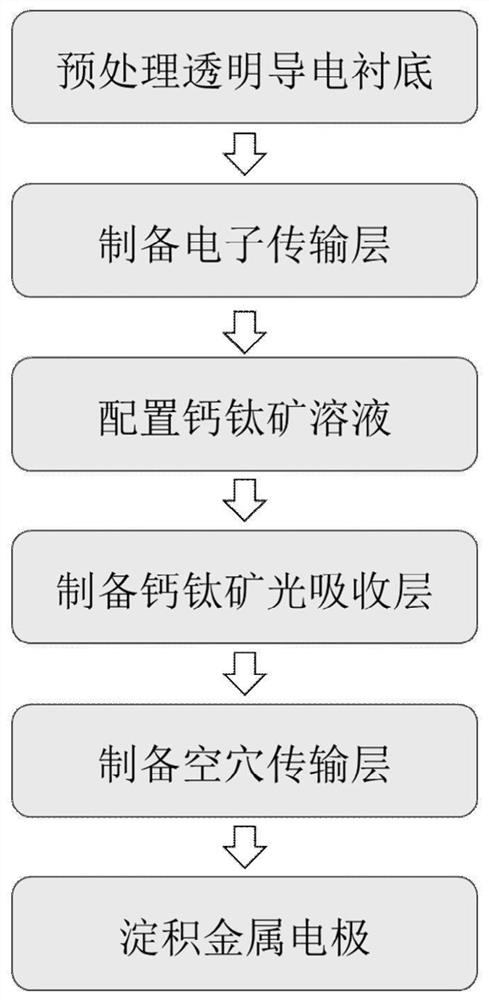
[0034] In the first step, the transparent conductive substrate ITO is selected and pretreated.
[0035] 1.1) Select indium tin oxide ITO transparent material as the conductive substrate;
[0036] 1.2) Ultrasonic cleaning the transparent conductive substrate with Decon-90 glass cleaning solution, deionized water, acetone, and isopropanol solution at a temperature of 50°C for 20 minutes each;
[0037] 1.3) Blow dry the glass surface of the transparent conductive substrate cleaned ultrasonically with nitrogen, and use ultraviolet ozone UV-zone to treat for 30 minutes to obtain the pretreated substrate; ...
Embodiment 2
[0050] Example 2: Preparation of transparent conductive substrate using fluorine-doped tin oxide FTO, electron transport layer using titanium dioxide TiO 2 , the perovskite light absorbing layer adopts Cs 2 AgBr x I 6-x , the hole transport layer uses 2,2,7,7-tetrakis[N,N-bis(4-methoxyphenyl)amino]-9,9-spiro-OMeTAD, and the top metal electrode uses Gold Au perovskite solar cells.
[0051] Step 1, select the transparent conductive substrate FTO, and perform pretreatment on it.
[0052] 1a) Select fluorine-doped tin oxide FTO transparent material as the conductive substrate;
[0053] 1b) Pretreatment of the conductive substrate
[0054] The specific implementation of this step is the same as 1.1) and 1.2) of Embodiment 1.
[0055] Step 2, prepare TiO 2 electron transport layer.
[0056] 2a) 0.2mol / L titanium dioxide TiO 2 The solution was spin-coated on the fluorine-doped tin oxide FTO substrate at a speed of 4000rpm for 45s, and then annealed at a temperature of 125°C ...
Embodiment 3
[0074] Example 3: Preparation of transparent conductive substrate using fluorine-doped tin oxide FTO, electron transport layer using tin dioxide SnO 2 , the perovskite light absorbing layer adopts Cs 2 InSbBr 6 , the hole transport layer uses copper thiocyanide CuSCN, and the top metal electrode uses copper Cu perovskite solar cells.
[0075] In step A, the transparent conductive substrate FTO is selected and pretreated.
[0076] The specific implementation of this step is the same as step 1 of embodiment 2.
[0077] Step B, preparation of SnO for perovskite solar cells 2 electron transport layer.
[0078] B1) 1mL of 15% tin dioxide SnO 2 The solution was dissolved in 2 mL of deionized water to obtain a concentration of 5% tin dioxide SnO 2 solution;
[0079] B2) SnO with a concentration of 5% 2 The solution was spin-coated on the pretreated FTO substrate at a speed of 5000 rpm for 30 seconds, and then annealed at a temperature of 150° C. for 30 minutes to obtain an el...
PUM
| Property | Measurement | Unit |
|---|---|---|
| thickness | aaaaa | aaaaa |
| thickness | aaaaa | aaaaa |
| thickness | aaaaa | aaaaa |
Abstract
Description
Claims
Application Information
 - R&D
- Intellectual Property
- Life Sciences
- Materials
- Tech Scout
- Unparalleled Data Quality
- Higher Quality Content
- 60% Fewer Hallucinations
Browse by: Latest US Patents, China's latest patents, Technical Efficacy Thesaurus, Application Domain, Technology Topic, Popular Technical Reports.
© 2025 PatSnap. All rights reserved.Legal|Privacy policy|Modern Slavery Act Transparency Statement|Sitemap|About US| Contact US: help@patsnap.com


