
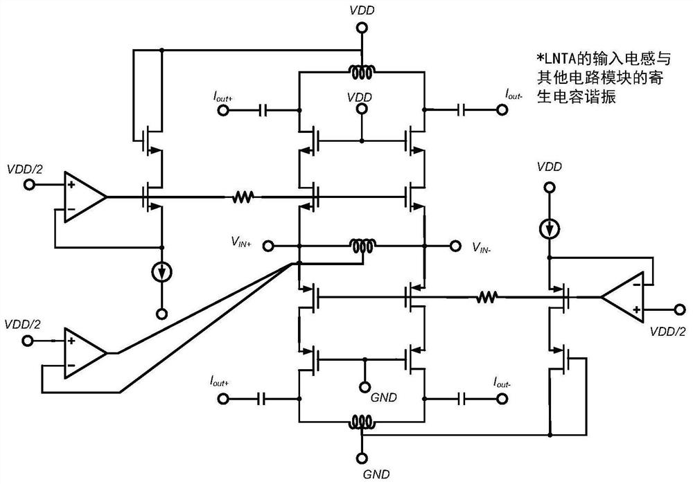
CMOS low-distortion low-noise amplifier circuit

A low-noise amplifier and low-distortion technology, applied in the direction of amplifiers, differential amplifiers, DC-coupled DC amplifiers, etc., can solve problems such as low power consumption and noise, and difficult large-signal interference environments

Pending Publication Date: 2020-11-13
CHENGDU UNIV OF INFORMATION TECH
View PDF2 Cites 10 Cited by
  • Summary
  • Abstract
  • Description
  • Claims
  • Application Information

AI Technical Summary

Problems solved by technology

In addition, the literature (Guo Benqing, A 8.1mW 0.1~2GHz inductorless CMOS LNTA for software-defined radio applications, IEEE ASICON, 1-4, 2015) proposed an innovative solution with low power consumption and noise, but the third-order Adjustment point linearity is below 0dBm, it is difficult to deal with large signal interference environment

Method used


Image

  • CMOS low-distortion low-noise amplifier circuit
  • CMOS low-distortion low-noise amplifier circuit
  • CMOS low-distortion low-noise amplifier circuit

Examples


Embodiment

[0047] The low noise amplifier circuit provided in this embodiment is realized by 180nm radio frequency CMOS technology, powered by 1.8V voltage, and the power consumption of the circuit is 18mW. Figure 6 The S11 simulation result diagram of the LNA is given, indicating that when S11 Figure 7 The noise figure result is given, and its minimum noise figure NF is about 2.84dB; Figure 8 The IIP3 simulation results in its band are given: the maximum value is 22.5dBm, and a two-tone test frequency interval of 10MHz is used here. It can also be seen that its power compression point P1dB>2.5dB; Figure 9 It is the simulation result graph of Blocker NF in the case of blocking interference, in P blocker =0dBm and 100MHZ frequency offset condition, the noise performance at 1GHz point frequency is NF=3.3dB; Figure 10 The gain curve of the low-noise amplifier is given, and it is noted that its voltage gain is 4dB, and the peak value of the transconductance gain reaches 100mS within th...


PUM


Abstract

The invention discloses a CMOS low-distortion low-noise amplifier circuit, which is applied to the field of radio frequency integrated circuits, and aims to solve the problems that the third-order intermodulation linearity of an amplifier circuit in the prior art is below 0dBm, and a large signal interference environment is difficult to deal with. The transconductance input stage adopts a complementary common-source stage structure, so that the current efficiency is doubled; the linearity improving stage adopts a complementary common-emitter stage to improve the small signal linearity of the complementary common-source stage; the feedback stage adopts a source follower to solve the second-order interaction problem of nonlinear active feedback; an off-chip element and an input parasitic capacitor form a [pi]-type matching network to enhance the input matching bandwidth, so that an on-chip high-capacity inductor is prevented from being used; and the common-mode feedback circuit detects common-mode voltage of an output port of the low-noise amplifier circuit and compares the common-mode voltage with a reference voltage, and an obtained error signal is in feedback connection with gridsof the Mp1 and the Mp2 through a bias resistor for dynamic adjustment, so that the circuit works at a stable direct-current working point.

Description

technical field [0001] The invention belongs to the field of radio frequency integrated circuits, in particular to a low noise amplifier circuit. Background technique [0002] At present, software wireless terminal technology is becoming more and more popular. It only needs to be configured at the baseband software protocol layer, and various standards that meet the requirements of different communication protocols can be flexibly compatible with each other and coexist on a set of hardware equipment platforms. Therefore, the research on broadband radio frequency transceiver technology is becoming more and more important. Compared with the traditional bloated transceiver structure, the new SAW (surface acoustic wave) filter-free transceiver structure proposed in recent years has quickly become the focus of the industry. In order to obtain good anti-jamming ability, the non-SAW receiver design abandons the traditional voltage mode and adopts a novel current mode design concep...

Claims


Application Information

Patent Timeline
IPC IPC(8): H03F1/26H03F3/45
CPCH03F1/26H03F3/45479
Inventor 郭本青陈鸿鹏邬经伟
Owner CHENGDU UNIV OF INFORMATION TECH
Learn More