A low noise amplifier

A low-noise amplifier and main body technology, applied in improving amplifiers to reduce noise impact, semiconductor devices, semiconductor/solid-state device manufacturing, etc., can solve the problems of high manufacturing cost, long transit time, and difficult process of passive devices, and achieve Improve interface defects, fast recovery speed, and good bendability

Active Publication Date: 2021-08-03
HUAZHONG UNIV OF SCI & TECH
View PDF11 Cites 0 Cited by
  • Summary
  • Abstract
  • Description
  • Claims
  • Application Information

AI Technical Summary

Problems solved by technology

[0007] Aiming at the defects and improvement needs of the prior art, the present invention provides a heterojunction bipolar transistor HBT and a low-noise amplifier including the HBT. There are a large number of defects in the heterojunction interface of the HBT-based low-noise amplifier LNA, which generates large noise, and the technical problems of high manufacturing cost and difficult process of passive devices

Method used


Image

  • A low noise amplifier
  • A low noise amplifier
  • A low noise amplifier

Examples


Embodiment Construction

[0045] In order to make the object, technical solution and advantages of the present invention clearer, the present invention will be further described in detail below in conjunction with the accompanying drawings and embodiments. It should be understood that the specific embodiments described here are only used to explain the present invention, not to limit the present invention. In addition, the technical features involved in the various embodiments of the present invention described below can be combined with each other as long as they do not constitute a conflict with each other.

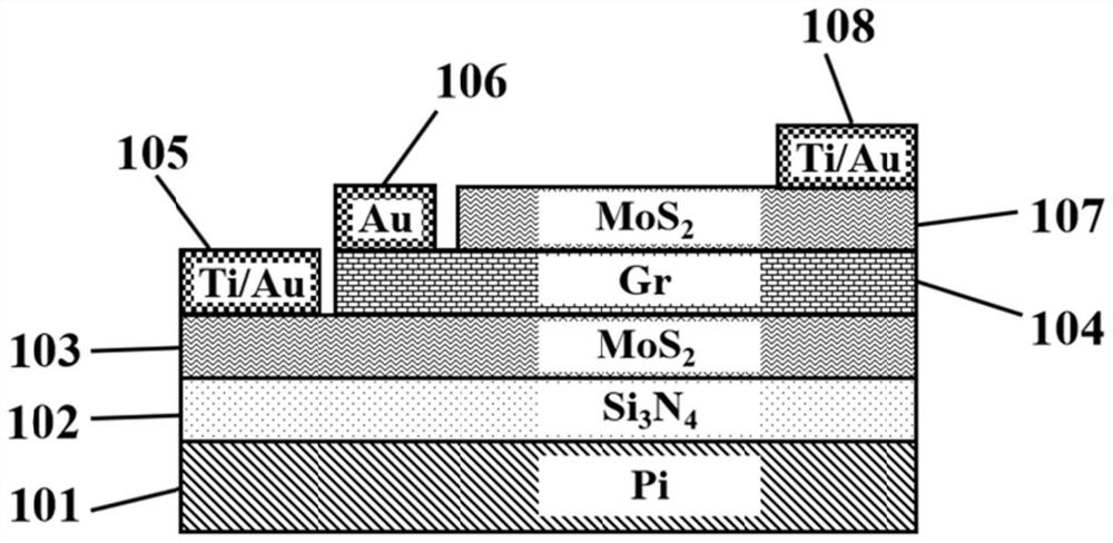
[0046] Such as figure 1 As shown, it is a schematic cross-sectional view of a heterojunction bipolar transistor HBT provided by the present invention, including: a substrate 101, a dielectric layer 102, an emitter body 103, a base body 104, and a collector Main body 107; The emitter main body 103 and the collector main body 107 are n-type two-dimensional transition metal sulfides, and the base ...


PUM


Abstract

The invention discloses a heterojunction bipolar transistor HBT and a low-noise amplifier including the HBT. The HBT includes: a substrate, a dielectric layer, an emitter body, a base body, and a collector body distributed sequentially from bottom to top ; The emitter body and the collector body are made of MoS 2 As a representative n-type two-dimensional transition metal sulfide, the base body is a p-type single-layer graphene Gr; it also includes: an emitter electrode, a base electrode, and a collector electrode; wherein, the emitter electrode and the The base body is on the emitter body, and the two are not in contact with each other; the base electrode and the collector body are on the base body, and the two are not in contact with each other; the collector electrode on the collector body. In the present invention, the HBT device part adopts two-dimensional materials to reduce the transit time; it has a Schottky barrier with smaller forward voltage drop and faster recovery speed; the passive device part adopts a coplanar waveguide structure, which can avoid Hole punching simplifies the process.

Description

technical field [0001] The invention belongs to the technical field of semiconductors, and in particular relates to a low-noise amplifier. Background technique [0002] As the process line width enters the atomic level of tens of nanometers, Moore's Law, which reflects the development law of silicon technology, will eventually become saturated. With the development of science and technology. Therefore, the International Semiconductor Technology Roadmap (ITRS) puts forward two main development directions of "More Moore" and "More than Moore". [0003] The development and application transformation of new materials can effectively promote the development of "More Moore" and "More than Moore". In the past decade, 2D materials have been extensively studied in various fields due to their excellent electrical, thermal, and mechanical properties. In addition, heterostructures based on 2D materials have attracted attention because of their weaker interlayer bonding, quantum effec...

Claims


Application Information

Patent Timeline
Patent Type & Authority Patents(China)
IPC IPC(8): H01L29/778H01L21/335H01L29/16H03F1/26
CPCH01L29/107H01L29/1606H01L29/66431H01L29/7786H03F1/26
Inventor 吴燕庆张誉宝李学飞
Owner HUAZHONG UNIV OF SCI & TECH
Why Eureka
Try Eureka