Manufacturing method of semiconductor device
A technology for semiconductors and devices, which is applied in the field of semiconductor preparation, can solve problems such as the top-layer metal interconnect layer hillock shape, and achieve the effects of avoiding weak electrical connections, suppressing thermal strain, and improving yield and reliability
- Summary
- Abstract
- Description
- Claims
- Application Information
AI Technical Summary
Problems solved by technology
Method used
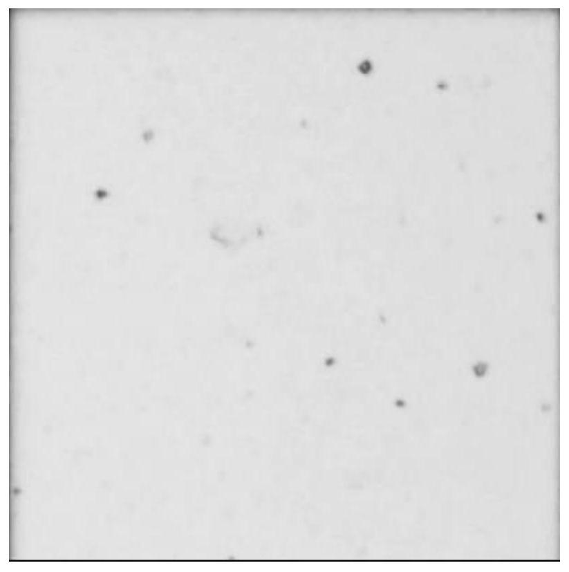
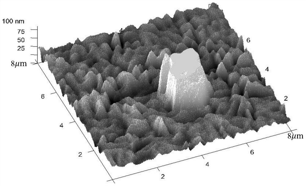
Image

Examples
preparation example Construction
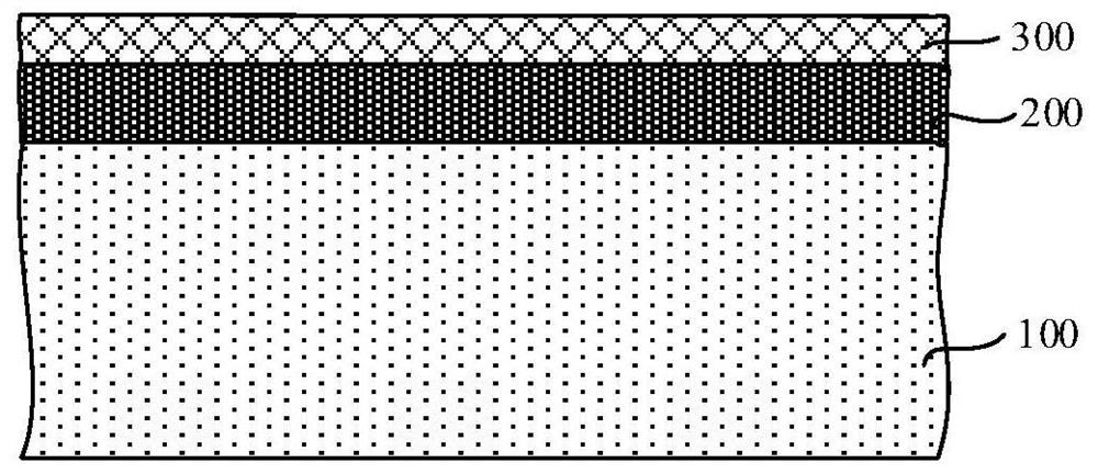
[0038] Figure 2a ~ Figure 2c It is a structural schematic diagram of corresponding steps in a method for preparing a semiconductor device. The fabrication method of the semiconductor device is as follows: Figure 2a As shown, a dielectric layer 200 and a top metal interconnect layer 300 are formed on the substrate 100; the top metal interconnect layer 300 is etched so that the top metal interconnect layer 300 has a set pattern; as Figure 2b As shown, a first passivation layer 401 and a second passivation layer 402 are sequentially formed on the top metal interconnection layer 300; Figure 2c As shown, the first passivation layer 401 and the second passivation layer 402 are etched to form an opening 500, and the opening 500 exposes part of the top metal interconnection layer 300 as a pad area.
[0039] Then a hydrogen passivation process is performed, which is to Figure 2c The wafer in the process is placed in a reaction chamber, and then the temperature of the reaction c...
PUM
 Abstract
Description
Claims
Application Information
 - Generate Ideas
- Intellectual Property
- Life Sciences
- Materials
- Tech Scout
- Unparalleled Data Quality
- Higher Quality Content
- 60% Fewer Hallucinations
Browse by: Latest US Patents, China's latest patents, Technical Efficacy Thesaurus, Application Domain, Technology Topic, Popular Technical Reports.
© 2025 PatSnap. All rights reserved.Legal|Privacy policy|Modern Slavery Act Transparency Statement|Sitemap|About US| Contact US: help@patsnap.com