Large-size YIG-doped single crystal thin film material and preparation method thereof
A single-crystal thin-film, large-size technology, applied in the direction of polycrystalline material growth, single crystal growth, single crystal growth, etc., can solve the problems of low production efficiency, small film size, narrow range of film saturation magnetization, etc., and achieve production efficiency Enhanced, well-matched lattice effects
- Summary
- Abstract
- Description
- Claims
- Application Information
AI Technical Summary
Problems solved by technology
Method used
Image

Examples
Embodiment 1
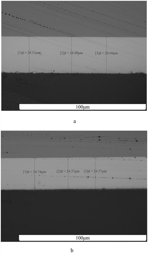
[0030] Fill the platinum crucible with Nd 2 o 3 (Weight 1.059g), Y 2 o 3 (weight 5.484g), Fe 2 o 3 (Weight 81.671g), B 2 o 3 (weight 17.302g), Ga 2 o 3 (weight 6.979g), PbO (weight 887.505g), heat up to 1100°C in the epitaxial furnace, keep it warm for 6 hours, and rotate the crucible forward and reverse in this state, so that the components can be uniformly soluteized, at 100°C Cool down at a rate of 1 hour, stabilize the temperature in a supersaturated state of 930°C, put the GGG substrate into the solution, rotate the substrate at a rate of 100 rpm, and perform ferrite single crystal thin film for 40 minutes at the same time grown to obtain a single crystal film with a thickness of 28.6 μm, which is complete without cracks and in a mirror state.
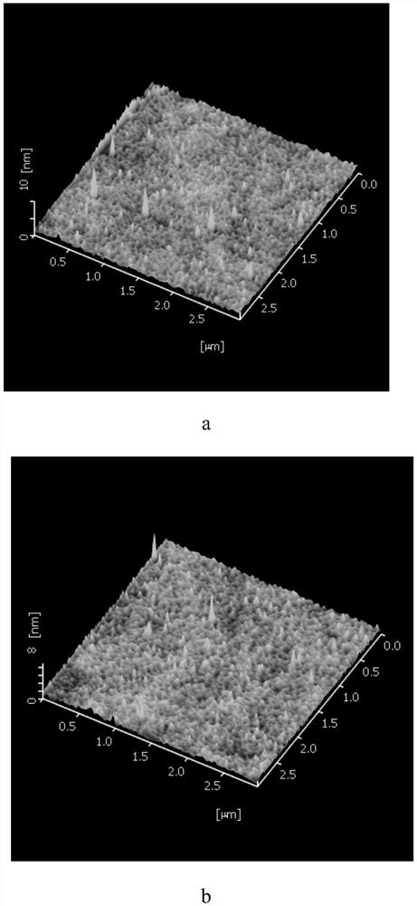
[0031] Using DPA (destructive physical analysis) to test the cross-section of the film, the thickness of the film is about 28.6 μm, as figure 1 As shown in -a; AFM (atomic force microscope) is used to detect the morpholo...
Embodiment 2
[0033] Fill the platinum crucible with Nd 2 o 3 (weight 0.826g), Y 2 o 3 (weight 5.668g), Fe 2 o 3 (weight 78.189g), B 2 o 3 (Weight 17.380g), Ge 2 o 3(weight 6.437g), PbO (weight 891.5g), heat up to 1100°C in the epitaxial furnace, keep it warm for 6 hours, and rotate the crucible forward and reverse in this state, so that the components can be uniformly soluteized, at 100°C Cool down at a rate of 920°C to stabilize the temperature at a rate of 920°C, put the GGG substrate into the solution, rotate the substrate at a rate of 100 rpm, and perform a ferrite single crystal thin film for 30 minutes at the same time grown to obtain a single crystal film with a thickness of 24.6 μm, which is complete without cracks and in a mirror state.
[0034] Using DPA (destructive physical analysis) to test the cross-section of the film, the thickness of the film is about 24.6 μm, as figure 1 As shown in -b; use AFM (atomic force microscope) to detect the morphology of the film in th...
Embodiment 3
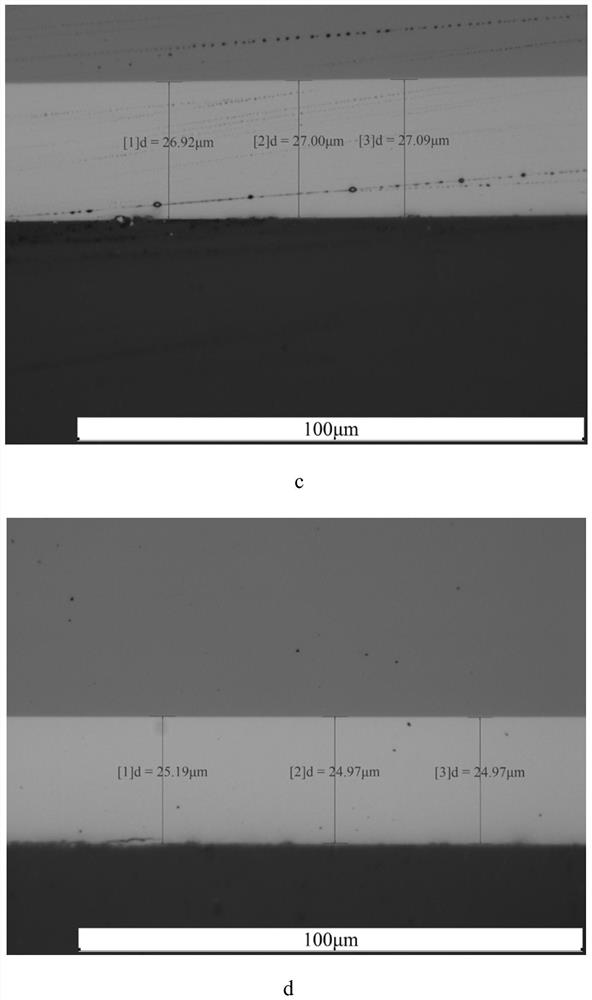
[0036] Fill the platinum crucible with La 2 o 3 (weight 1.276g), Y 2 o 3 (weight 5.315g), Fe 2 o 3 (Weight 86.114g), B 2 o 3 (Weight 17.314g), Ga 2 o 3 (weight 1.838g), PbO (weight 888.143g), heat up to 1100°C in the epitaxial furnace, keep it warm for 6 hours, and rotate the crucible forward and reverse in this state, so that the substances of each component can be uniformly soluteized, at 100°C Cool down at a rate of 1 hour, stabilize the temperature in a supersaturated state of 940°C, put the GGG substrate into the solution, rotate the substrate at a rate of 100 rpm, and perform ferrite single crystal thin film for 40 minutes at the same time grown to obtain a single crystal film with a thickness of 27.1 μm, which is complete without cracks and in a mirror state.
[0037] Using DPA (destructive physical analysis) to test the cross-section of the film, the thickness of the film is about 27.1 μm, such as figure 1 As shown in -c; use AFM (atomic force microscope) to ...
PUM
| Property | Measurement | Unit |
|---|---|---|
| thickness | aaaaa | aaaaa |
| surface roughness | aaaaa | aaaaa |
| thickness | aaaaa | aaaaa |
Abstract
Description
Claims
Application Information
 - R&D
- Intellectual Property
- Life Sciences
- Materials
- Tech Scout
- Unparalleled Data Quality
- Higher Quality Content
- 60% Fewer Hallucinations
Browse by: Latest US Patents, China's latest patents, Technical Efficacy Thesaurus, Application Domain, Technology Topic, Popular Technical Reports.
© 2025 PatSnap. All rights reserved.Legal|Privacy policy|Modern Slavery Act Transparency Statement|Sitemap|About US| Contact US: help@patsnap.com