
Method for converting high-temperature reverse bias aging time of crimping type insulated gate bipolar transistor

A technology of bipolar transistors and aging time, applied in calculation, computer-aided design, CAD circuit design, etc., can solve the problems of accelerated aging model, lack of passivation layer insulation life impact, waste, etc.

Active Publication Date: 2020-10-30
NORTH CHINA ELECTRIC POWER UNIV (BAODING)
View PDF2 Cites 0 Cited by
  • Summary
  • Abstract
  • Description
  • Claims
  • Application Information

AI Technical Summary

Problems solved by technology

At present, there is a lack of a clear accelerated aging model for the terminal of the press-fit IGBT device, especially the lack of analysis of the impact of mechanical stress on the insulation life of the passivation layer at the device terminal
[0008] The above-mentioned deficiencies will make it difficult to reasonably determine the endurance test time of the press-connected IGBT chip, and it is difficult to convert the test results under standard test conditions to various application scenarios of different temperatures, electric fields, and mechanical stress.
If products are screened according to the most stringent application scenarios, it will cause great waste and high cost

Method used


Image

  • Method for converting high-temperature reverse bias aging time of crimping type insulated gate bipolar transistor
  • Method for converting high-temperature reverse bias aging time of crimping type insulated gate bipolar transistor
  • Method for converting high-temperature reverse bias aging time of crimping type insulated gate bipolar transistor

Examples


Embodiment Construction

[0037] Taking a 3300V / 50A single-chip crimp IGBT device as an example, the specific implementation of the present invention will be described in detail below.

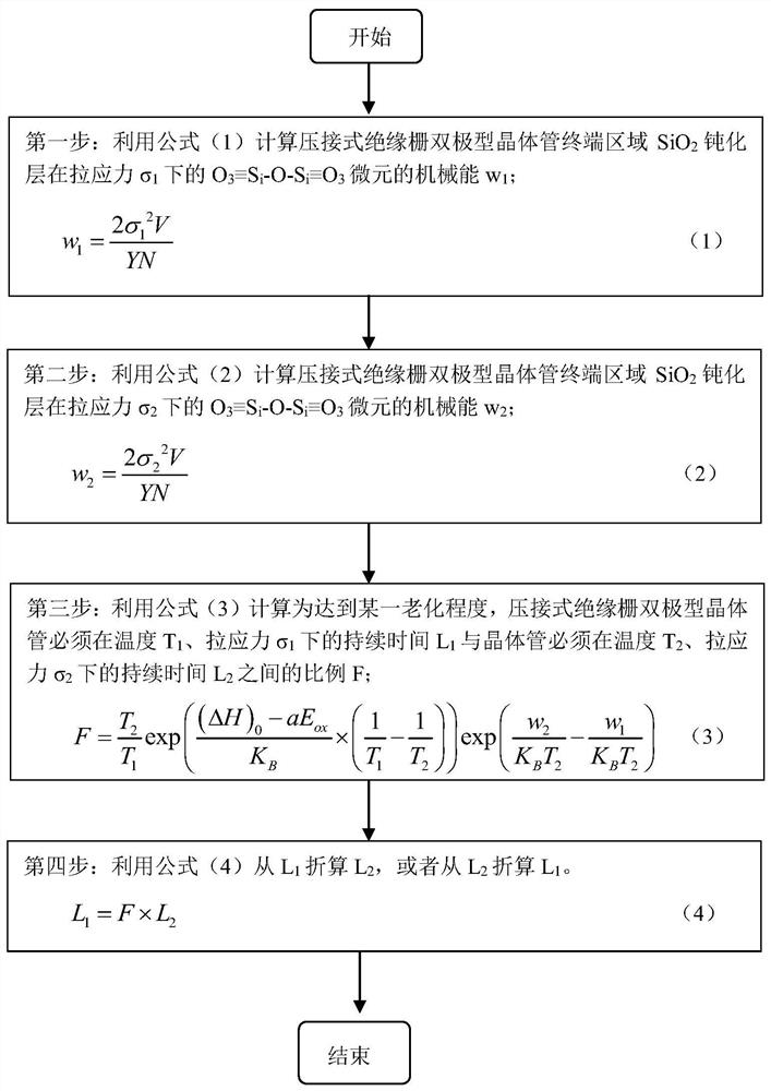
[0038] It is known that under the clamping force of the crimping IGBT, the maximum tensile stress of the passivation layer is 67.1Mpa; when a mechanical pressure of 2Gpa is applied, the maximum tensile stress of the passivation layer reaches 2.8Gpa, and the electric field strength on the passivation layer in the terminal area is as high as 200kV / cm. When a certain type of press-connect IGBT is subjected to a high-temperature reverse bias test, the temperature T 1 is 423K, the device is subjected to external mechanical pressure (the pressure is kept at 2Gpa, then the maximum tensile stress σ of the passivation layer 1 Reach 2.8Gpa), get the accelerated aging life of the device L f-test 200 hours, it is necessary to calculate the actual working conditions (temperature T 2 is 323K, the maximum tensile stress σ of the p...


PUM

PropertyMeasurementUnit
elastic modulusaaaaaaaaaa
strengthaaaaaaaaaa

Abstract

The invention discloses a method for converting high-temperature reverse bias aging time of a crimping type insulated gate bipolar transistor. The method comprises the following steps: calculating mechanical energy in a material infinitesimal element caused by tensile stress of a passivation layer in a terminal region of the crimping type IGBT device to obtain the proportionality coefficient of the aging time which must be continued under different temperatures and mechanical pressures for the same aging degree of the IGBT device, so that the conversion between different aging times is realized, and the conversion between the accelerated aging life of the device under the test condition and the service life of the device under the actual working condition can be realized.

Description

technical field [0001] The invention belongs to the field of reliability test methods for power electronic devices, and relates to the determination and detection of the high-temperature reverse bias test time of a high-power insulated gate bipolar transistor (IGBT), in particular to the pressure-connected IGBT device passivation layer under different temperatures and mechanical stresses. The following aging time conversion method. Background technique [0002] In recent years, a new package form of high-power insulated-gate bipolar transistor (IGBT) devices—crimping type—appears. The unique design of high-power press-fit IGBT devices has no leads, no soldering, and double-sided heat dissipation, which greatly improves the power capacity of a single device and improves device reliability. At present, it has a tendency to replace traditional welding potting IGBT devices. Become one of the preferred devices for high-end applications. Unlike previous soldered packages, press-...

Claims


Application Information

Patent Timeline
Patent Type & Authority Applications(China)
IPC IPC(8): G06F30/39G06F119/04
Inventor 程养春郑夏晖
Owner NORTH CHINA ELECTRIC POWER UNIV (BAODING)
Learn More