Laser boron-doped back passivation solar cell and preparation method thereof
A solar cell and boron doping technology, applied in the field of solar cells, can solve the problems of decreased passivation capability, lower back interface state, lower cell conversion efficiency, etc.
- Summary
- Abstract
- Description
- Claims
- Application Information
AI Technical Summary
Problems solved by technology
Method used
Image
Examples
Embodiment 1
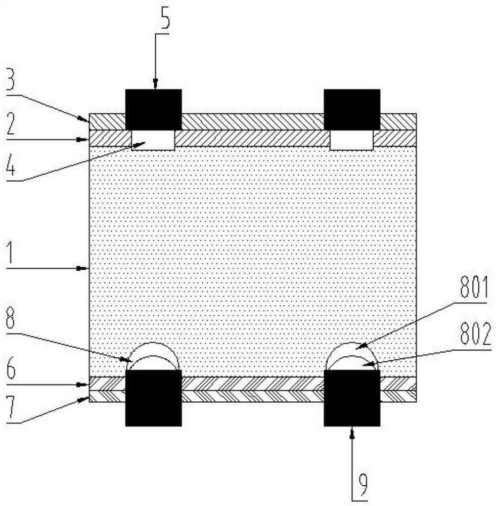
[0034] refer to figure 2 , the present embodiment provides a laser boron-doped back-passivated solar cell, comprising P-type silicon 1, and the front side of the P-type silicon 1 is sequentially provided with a phosphorus-doped layer 2 (N+ layer), SiN x The anti-reflection layer 3 and the Ag grid finger electrode 5 are passivated on the front side, and a heavily doped silicon layer 4 (N++ layer) is also provided on the front side of the P-type silicon 1, and the Ag grid finger electrode 5 is connected with the heavily doped silicon layer 4 and The upper surface of the P-type silicon 1 is connected, and the back of the P-type silicon 1 is sequentially provided with AlO x Passivation layer 6, SiN x The back passivates the anti-reflection layer 7 and the Al gate finger electrode 9, and the back side of the P-type silicon 1 is also provided with a heavily doped region 8, and the heavily doped region 8 includes a boron heavily doped layer 801 (P++ layer) and a local Contact the ...
Embodiment 2
[0036] This embodiment provides a method for preparing a laser boron-doped back passivated solar cell, comprising the following steps:
[0037] (1) Alkali texture is used to remove the damaged layer of the silicon wafer in the tank and texture it to form a pyramid texture with a height of 0.5 μm-5 μm;
[0038] (2) Using phosphorus oxychloride (POCl 3 ) high-temperature diffusion, the reaction temperature is 750-850°C, and the reaction time is 30-60min, forming a phosphorus-doped layer on the surface of the silicon wafer, that is, a P-doped N+ emitter junction;
[0039] (3) Laser doping is used to form a heavily doped silicon layer (N++ layer);
[0040] (4) Using wet etching process, with HNO 3 / HF mixed solution, remove the P-doped N+ junction on the back of the silicon wafer, and polish the back, high temperature annealing, the annealing reaction temperature is 750-850 °C;
[0041](5) AlO is sequentially deposited on the back of the silicon wafer by atomic layer deposition...
Embodiment 3
[0047] This embodiment is preferred on the basis of embodiment 2, the AlO x layer was prepared using TMA and O 2 / N 2 A mixed gas of O, the reaction temperature is 200-350°C, and the thickness is 5-15nm;
[0048] The SiN x layer using SiH 4 and NH 3 mixed gas, the reaction temperature is 300-550°C, the thickness is 70-110nm, and the refractive index is 1.9-2.2. The SiN x Layers can be single or double or triple layered.
PUM
| Property | Measurement | Unit |
|---|---|---|
| thickness | aaaaa | aaaaa |
| thickness | aaaaa | aaaaa |
| particle diameter | aaaaa | aaaaa |
Abstract
Description
Claims
Application Information
 - Generate Ideas
- Intellectual Property
- Life Sciences
- Materials
- Tech Scout
- Unparalleled Data Quality
- Higher Quality Content
- 60% Fewer Hallucinations
Browse by: Latest US Patents, China's latest patents, Technical Efficacy Thesaurus, Application Domain, Technology Topic, Popular Technical Reports.
© 2025 PatSnap. All rights reserved.Legal|Privacy policy|Modern Slavery Act Transparency Statement|Sitemap|About US| Contact US: help@patsnap.com


