Semiconductor device

A semiconductor and conductive pattern technology, applied in the direction of semiconductor devices, semiconductor/solid-state device components, output power conversion devices, etc., can solve problems such as oscillation

Pending Publication Date: 2020-10-20
FUJI ELECTRIC CO LTD
View PDF11 Cites 0 Cited by
  • Summary
  • Abstract
  • Description
  • Claims
  • Application Information

AI Technical Summary

Problems solved by technology

[0004] In addition, in the structure where IGBT elements are connected in parallel, oscillation may occur during switching operation due to conditions such as the gate capacitance of the IGBT elements, the inductance between the IGBT elements connected in parallel, and the inductance between the IGBT gates.

Method used


Image

  • Semiconductor device
  • Semiconductor device
  • Semiconductor device

Examples


Embodiment Construction

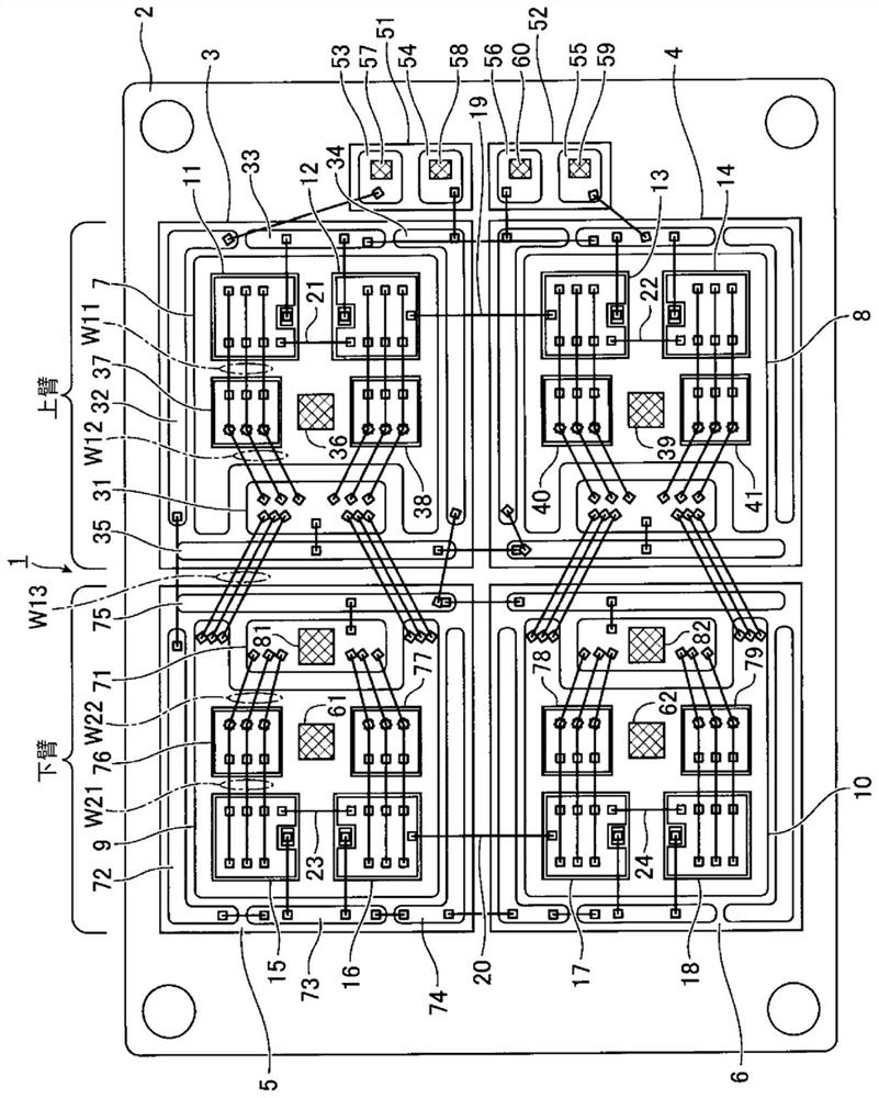
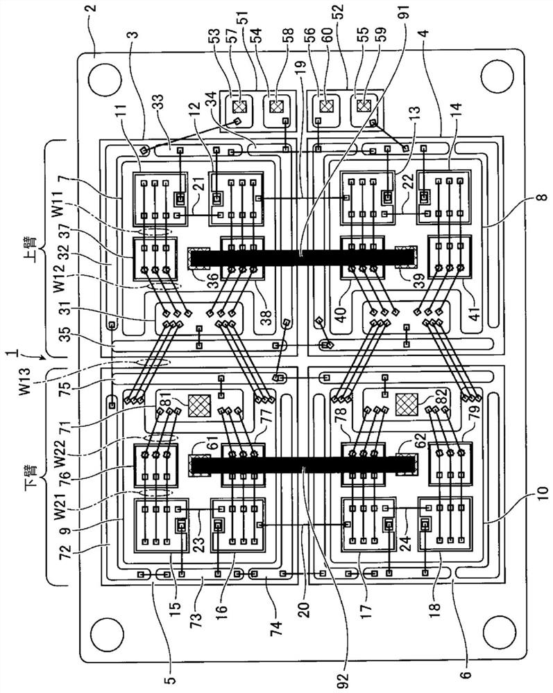
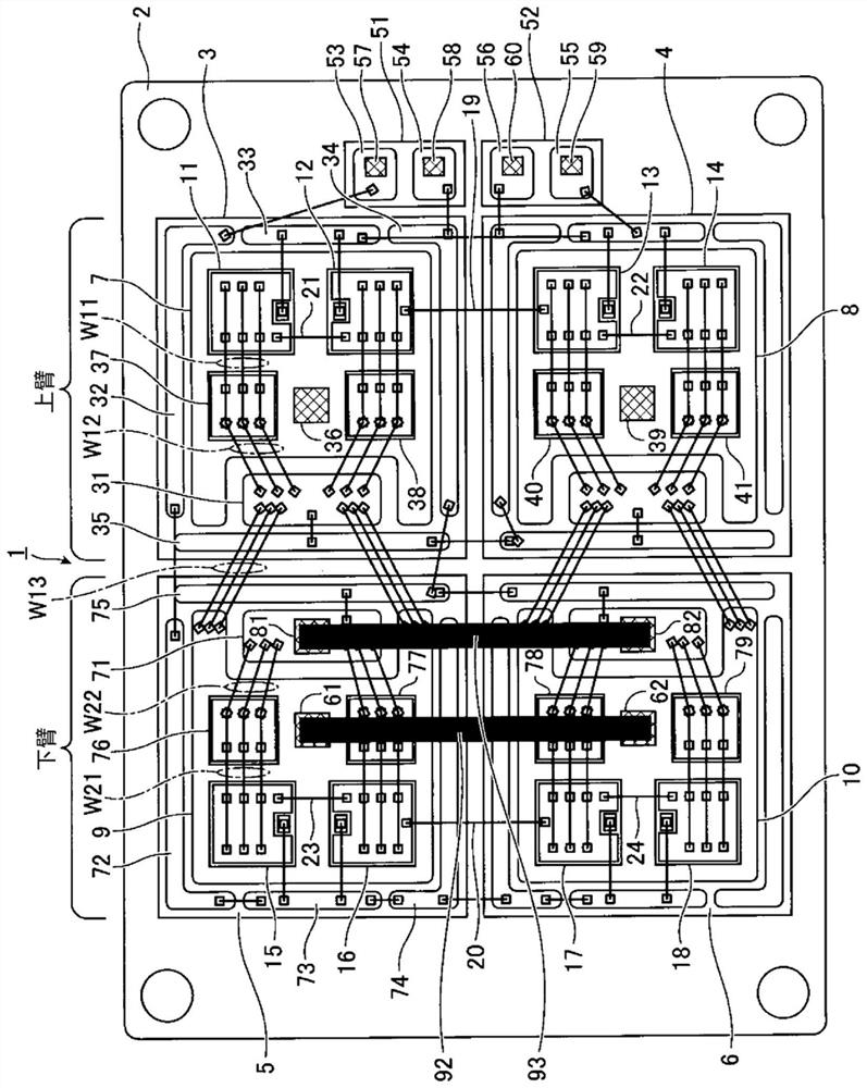
[0027] Next, an example in which the semiconductor device according to the present embodiment is applied to a power module of an inverter circuit will be described, but the semiconductor device is not limited to the inverter circuit. As long as it is a power module having a structure in which power switching elements arranged on different conductive patterns are connected in parallel, the semiconductor device of this embodiment can also be applied to circuits other than inverter circuits. In addition, in this embodiment, an example in which an IGBT element is used as a switching element is described, but a power switching element other than an IGBT element can be used as a switching element. For example, a MOSFET (Metal Oxide Semiconductor Field Effect Transistor: Metal Oxide Semiconductor Field Effect Transistor) element may be used instead of the IGBT element. In the case of a MOSFET element, the emitter electrode is replaced by a source electrode for reading, and the collec...


PUM


Abstract

The present invention suppresses an oscillation phenomenon during a switching operation even in a configuration where switching elements are arranged on different conductive patterns and are connectedin parallel. A semiconductor device (1) is provided with: substrates (3-6) that have main surfaces; a plurality of conductive patterns (7-10) that are arranged on the main surfaces; a plurality of switching elements (11-18) that are arranged so as to connect collector electrodes on the conductive patterns; and one or more wiring members (19, 20) that directly connect emitter electrodes of the switching elements, arranged on the different conductive patterns and connected in parallel, among the switching elements.

Description

technical field [0001] The invention relates to a semiconductor device having a plurality of switching elements. Background technique [0002] There is a semiconductor device using a power semiconductor element as a switching element in a power conversion device used in new energy fields such as wind power and solar power generation, and in the vehicle field. For example, in a semiconductor device for power conversion, an IGBT (Insulated Gate Bipolar Transistor: Insulated Gate Bipolar Transistor) excellent in high voltage, high current, and high-speed switching operation is used as a switching element. [0003] A semiconductor device using an IGBT element as a switching element will be described as an example. For example, in a semiconductor device for power conversion, a power module composed of an upper arm and a lower arm is provided between a high power supply potential (P) and a low power supply potential (N). In a power module, when an IGBT element is used as a switc...

Claims


Application Information

Patent Timeline
Patent Type & Authority Applications(China)
IPC IPC(8): H01L25/07H01L23/48H01L25/18H02M7/48
CPCH01L25/18H01L2224/40137H01L2224/49111H01L2224/48139H01L2224/49113H01L2924/19107H02M7/003H02M7/219H01L23/49811H01L23/49844H01L25/072H01L2224/0603H01L2224/48137H01L2224/4846H01L2224/45015H01L2224/45144H01L2224/45147H01L2224/45124H01L24/45H01L2224/29101H01L2224/83801H01L2224/32225H01L2224/73265H01L2924/20751H01L2924/20752H01L2924/20753H01L2924/20754H01L2924/20755H01L2924/20756H01L2924/20757H01L2924/20758H01L2924/20759H01L2924/2076H01L2924/00014H01L2924/014H01L2224/48227H01L2924/00H01L24/48H01L2924/12036H01L2924/13055H01L2924/14252
Inventor 堀江峻太岩本进
Owner FUJI ELECTRIC CO LTD
Why Eureka
Try Eureka