
Semiconductor package

一种半导体、存储器的技术,应用在半导体器件、半导体/固态器件制造、半导体/固态器件零部件等方向,能够解决处理数据所需时间画面延迟等问题

Pending Publication Date: 2020-10-09
POWERCHIP SEMICON MFG CORP
View PDF16 Cites 0 Cited by
  • Summary
  • Abstract
  • Description
  • Claims
  • Application Information

AI Technical Summary

Problems solved by technology

[0003] Recently, as users have higher and higher requirements for display quality (such as image resolution, color saturation, etc.), the driver needs to process more and more data, which may be due to the time required for data processing. Defect (mura) caused by picture delay caused by too long

Method used


Image

  • Semiconductor package
  • Semiconductor package

Examples


Embodiment Construction

[0042] The present invention will be described more fully with reference to the accompanying drawings of this embodiment. However, the present invention can also be embodied in various forms and should not be limited to the embodiments described herein. In the drawings, the thicknesses of layers and regions may be exaggerated for clarity. The same or similar reference numerals denote the same or similar elements, and the following paragraphs will not repeat them one by one.

[0043] It will be understood that when an element is referred to as being “on” or “connected to” another element, it can be directly on or connected to the other element or intervening elements may also be present. When an element is referred to as being "directly on" or "directly connected to" another element, there are no intervening elements present. As used herein, "connected" may refer to a physical and / or electrical connection, while "electrically connected" or "coupled" may refer to the presence ...


PUM


Abstract

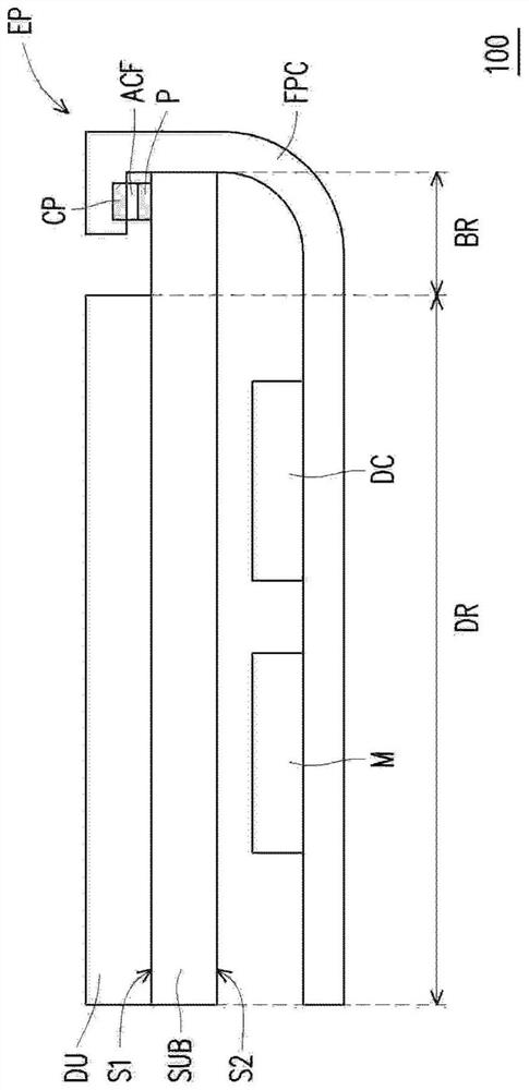
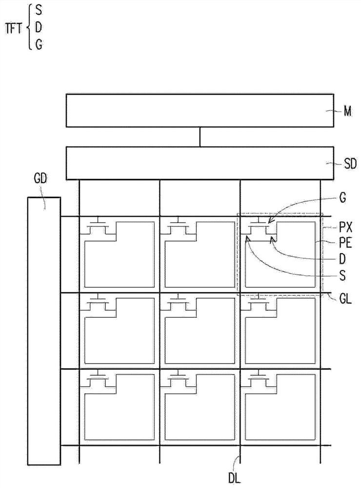
The present disclosure provides a semiconductor package including a substrate, a display unit, a flexible substrate, a driving circuit, and a memory. The substrate has a first surface and a second surface opposite to each other, and the first surface has a display region and a bonding region. The display unit is disposed on the display region of the first surface. The flexible substrate is disposed below the second surface and has a connection portion extended to the bonding region of the first surface. The driving circuit is disposed on the flexible substrate and electrically connects with the display unit. The memory is disposed on the flexible substrate and electrically connects with the driving circuit.

Description

technical field [0001] The present invention relates to a package structure, and in particular to a semiconductor package. Background technique [0002] With the continuous advancement of display technology, there is an increasing demand for a driver (also called driver IC) with a highly integrated integrated circuit (IC) that can drive the display after being connected. Therefore, various semiconductor packages have been developed. In general, common semiconductor packages for driving display units can be, for example, Chip On Glass (COG), Tape Carrier Package (TCP) and Chip On Film (COF) . Compared with COG, TCP and COF can make the display have a narrow frame design, so they are often used to drive the semiconductor package of the display unit. However, as the demand for drivers with small size and / or high operating speed gradually increases, TCP has been gradually replaced by COF because of its inferior line pitch or joint space as COF. [0003] Recently, as users hav...

Claims


Application Information

Patent Timeline
Patent Type & Authority Applications(China)
IPC IPC(8): H01L51/52G02F1/1345G09F9/35
CPCG02F1/13452G09F9/35H01L23/5387H01L25/0655H05K1/189H05K1/147H05K3/323H05K2201/10128H01L25/18H05K1/183H01L2924/12041H01L2924/12044H01L2924/1438H01L2924/1451H01L2924/1431H01L24/05H01L2924/14511H01L2924/1437H01L2924/1436
Inventor 陈俊良许汉杰
Owner POWERCHIP SEMICON MFG CORP
Learn More