Tellurene-based polarized light photoelectric detector and preparation method and application thereof
A photodetector and polarized light technology, applied in the direction of circuits, electrical components, semiconductor devices, etc., to achieve the effect of simple steps, efficient detection, and high detection limit
- Summary
- Abstract
- Description
- Claims
- Application Information
AI Technical Summary
Problems solved by technology
Method used
Image
Examples
Embodiment 1
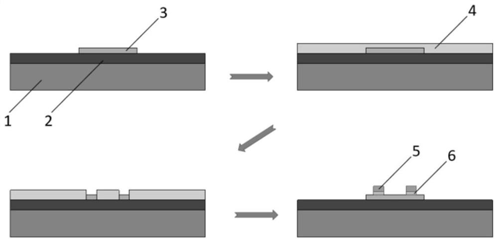
[0041] Such as figure 2 Shown, a kind of preparation method of polarized light photodetector based on tellurene, this method comprises the following steps:
[0042] Substrate preparation: use a silicon wafer knife to cut a commercial standard 4-inch p-type doped single-polished silicon oxide wafer (the thickness of the silicon part is 500um, the resistivity is 1-10Ω·cm, SiO 2 Thickness is 285nm) cut into 1×1cm 2 size. Afterwards, soak in acetone solution and isopropanol solution, ultrasonicate for 5 minutes respectively, and then blow dry with nitrogen to obtain a silicon wafer substrate.
[0043] Sample preparation: Tellurene is stored in ethanol solution. After ultrasonicating the tellurene stored in ethanol solution for 1 minute, use a dropper to take 3 drops onto the silicon wafer substrate prepared in the substrate preparation step, and use Blow dry with nitrogen.
[0044] Uniform glue drying: Spin-coat photoresist PMMA A4 on the above-mentioned silicon wafer substra...
Embodiment 2
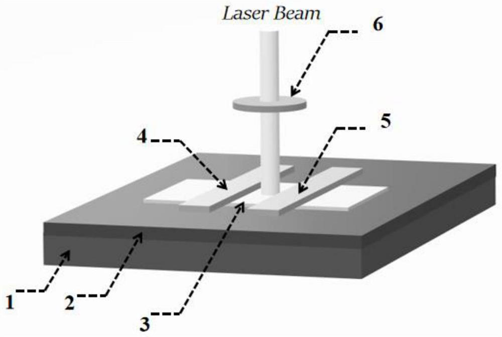
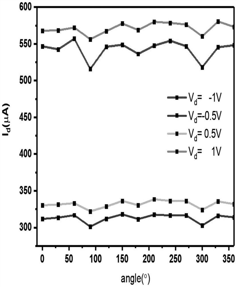
[0048] A test method for linearly polarized light detection based on tellurene polarized light photodetectors, the method comprising the following steps:
[0049] (1) Take the tellurene-based polarized light photodetector prepared in Example 1, and cut the silicon dioxide layer with a silicon wafer at a corner of the surface of the silicon wafer.
[0050] (2) Use a semiconductor characteristic analyzer to perform the test, place the silicon wafer on the supporting probe platform, and find the exact position of the detector on the silicon wafer through the CCD imaging system.
[0051] (3) Operate the probe movement knob of the probe platform, so that the three probes respectively contact the source and drain electrodes of the detector, and the silicon dioxide layer cut in step (1) (as the back gate electrode of the detector) .
[0052] (4) Run the test software of the semiconductor characteristic analyzer, select the voltage scanning mode for the drain probe, the scanning rang...
PUM
| Property | Measurement | Unit |
|---|---|---|
| thickness | aaaaa | aaaaa |
| thickness | aaaaa | aaaaa |
| thickness | aaaaa | aaaaa |
Abstract
Description
Claims
Application Information
 - Generate Ideas
- Intellectual Property
- Life Sciences
- Materials
- Tech Scout
- Unparalleled Data Quality
- Higher Quality Content
- 60% Fewer Hallucinations
Browse by: Latest US Patents, China's latest patents, Technical Efficacy Thesaurus, Application Domain, Technology Topic, Popular Technical Reports.
© 2025 PatSnap. All rights reserved.Legal|Privacy policy|Modern Slavery Act Transparency Statement|Sitemap|About US| Contact US: help@patsnap.com


