Device and process for packaging UVC LED chip on wafer

A chip and wafer technology, applied in the field of packaging devices, can solve problems such as damage to wafer circuits, and achieve the effect of facilitating wafer slotting

Active Publication Date: 2020-09-08
SHENZHEN CHANGFANG GRP CO LTD
View PDF9 Cites 5 Cited by
  • Summary
  • Abstract
  • Description
  • Claims
  • Application Information

AI Technical Summary

Problems solved by technology

[0004] Based on the technical problem that the grinding of the existing device for packaging UVC LED chips on the wafer easily causes damage to the wafer circuit, the present invention proposes a device for packaging UVC LED chips on the wafer

Method used


Image

  • Device and process for packaging UVC LED chip on wafer
  • Device and process for packaging UVC LED chip on wafer
  • Device and process for packaging UVC LED chip on wafer

Examples


Embodiment 1

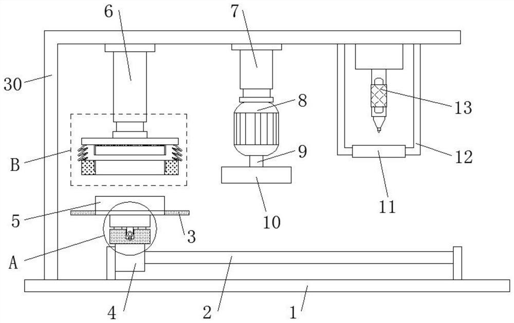
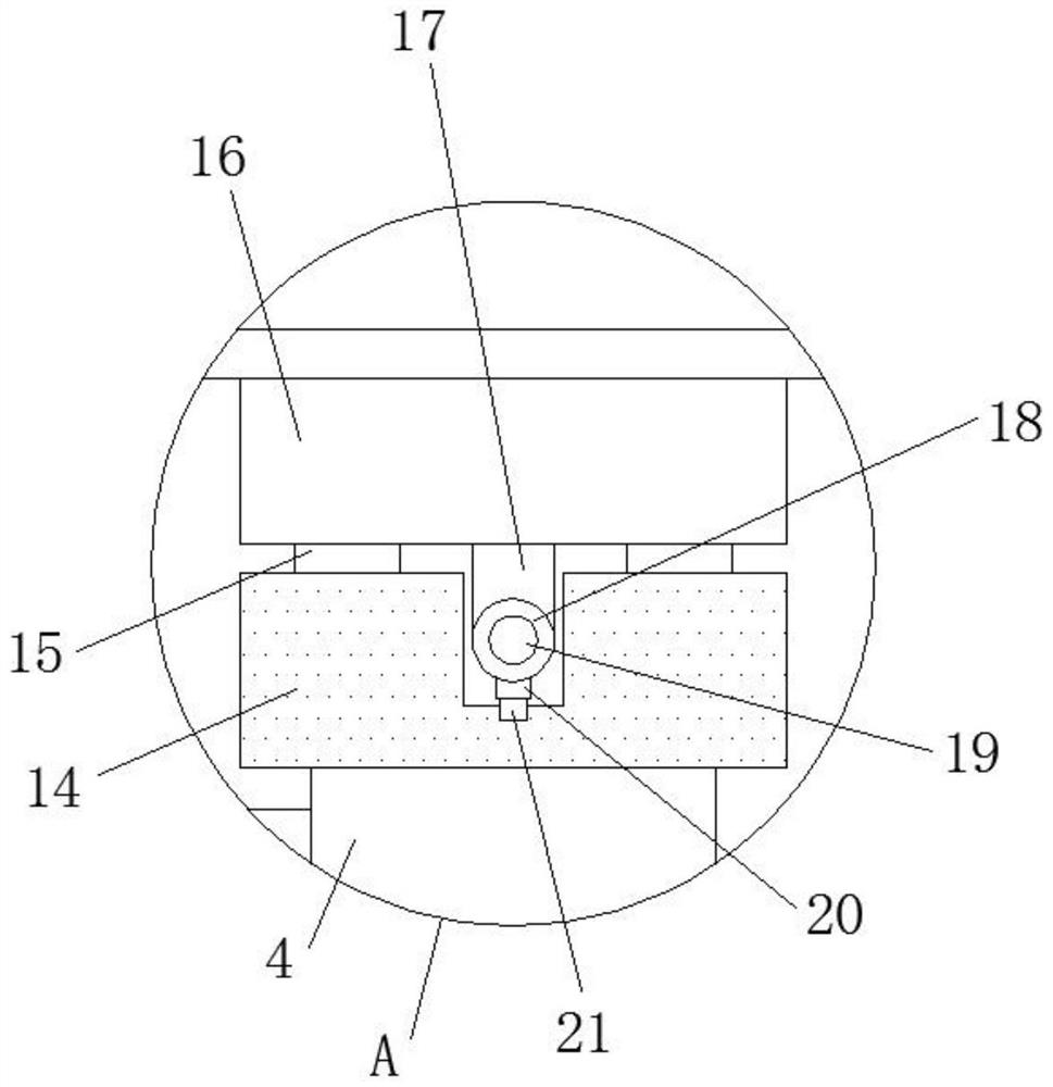
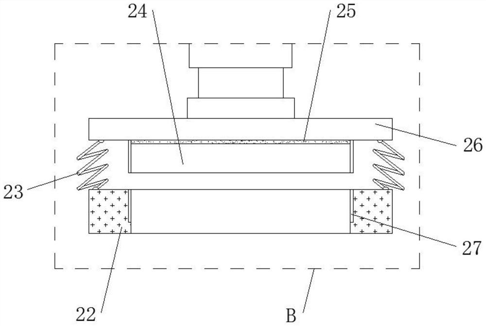
[0026] refer to Figure 1-4 , a device for packaging UVC LED chips on a wafer, including a base plate 1 and an L-shaped frame 30, the L-shaped frame 30 is fixed on the top outer wall of the base plate 1 by bolts, and the L-shaped frame 30 is inverted, and the base plate 1 An electric slide rail 2 is fixed on the outer wall of the top by bolts, and a slider 4 is slidably connected to one side of the outer wall of the electric slide rail 2. The first electric telescopic rod 6 is fixed by bolts, and one end of the extension rod of the first electric telescopic rod 6 is provided with a coating mechanism. Rod 7, one end of the extension rod of the second electric telescopic rod 7 is fixed with a micromotor 8 by a bolt, and one end of the output shaft of the micromotor 8 is keyed to a transmission shaft 9, and a grinding wheel 10, L A slotting mechanism is provided at a position close to the second electric telescopic rod 7 on the top inner wall of the jig 30 .

[0027] In the pre...

Embodiment 2

[0032] refer to Figure 5 , a device for packaging UVC LED chips on a wafer. Compared with Embodiment 1, this embodiment has a riser 28 fixed on the bottom outer wall of the bottom plate 1 close to the electric slide rail 2 through bolts, and the riser 28 is close to the electric slide rail. 2 is fixed with hot blower 29 by bolt on the one side outer wall.

[0033] When in use, after the operation is completed, the hot air blower 29 can be started for slight blowing, and the rising hot air is used to dry the wafer by using the principle of rising hot air, so as to avoid direct drying.


PUM


Abstract

The invention discloses a device and process for packaging a UVC LED chip on a wafer. Directed at the problem that a wafer line is prone to being damaged, the invention puts forward the following scheme that: the device comprises a bottom plate and an L-shaped frame, the L-shaped frame is fixed to the outer wall of the top of the bottom plate through bolts, the L-shaped frame is inverted, an electric sliding rail is fixed to the outer wall of the top of the bottom plate through bolts, a sliding block is slidably connected to the outer wall of one side of the electric sliding rail, a supportingplatform mechanism is arranged on the outer wall of the top of the sliding block, a first electric telescopic rod is fixed to one side of the inner wall of the top of the L-shaped frame through bolts, a film covering mechanism is arranged at one end of an extension rod of the first electric telescopic rod, and a second electric telescopic rod is fixed to a position, close to the first electric telescopic rod, of the inner wall of the top of the L-shaped frame. According to the invention, a paster and a wafer are rapidly laminated and cut, and the surface of the wafer is completely covered after the paster and the wafer are laminated, thereby facilitating the subsequent wafer grinding, avoiding the damage of a wafer line, and facilitating the slotting and packaging of the wafer.

Description

technical field [0001] The invention relates to the technical field of packaging devices, in particular to a device and process for packaging UVC LED chips on a wafer. Background technique [0002] Wafer refers to the substrate (also called substrate) on which semiconductor transistors or integrated circuits are manufactured. Because it is a crystalline material, its shape is round, so it is called a wafer. Substrate materials include silicon, germanium, etc. Since silicon is the most commonly used, if the crystal material is not specified, it usually refers to a silicon wafer. On-wafer packaging usually uses germicidal ultraviolet diodes, that is, UVC LEDs. The packaging process requires grinding and slotting, so it needs to be used on the wafer. A device for packaging UVC LED chips. [0003] At present, most of the existing devices for packaging UVC LED chips on the wafer in the market have the following disadvantages: it is very easy to cause damage to the wafer circui...

Claims


Application Information

Patent Timeline
Patent Type & Authority Applications(China)
IPC IPC(8): H01L21/67H01L21/683H01L33/48
CPCH01L21/67092H01L21/6835H01L33/48H01L2221/68327H01L2933/0033
Inventor 刘志刚王敏胡丰森江玮饶奋明
Owner SHENZHEN CHANGFANG GRP CO LTD
Why Eureka
Try Eureka