A display substrate and its preparation method

A technology for displaying substrates and substrates, applied in semiconductor devices, electrical components, circuits, etc., can solve problems such as short circuit between cathode and anode of electrode materials, and achieve the effect of improving electrode binding quality, improving quality, and ensuring firmness

Active Publication Date: 2022-07-12
BOE TECH GRP CO LTD
View PDF2 Cites 0 Cited by
  • Summary
  • Abstract
  • Description
  • Claims
  • Application Information

AI Technical Summary

Problems solved by technology

[0004] The invention provides a display substrate and a preparation method thereof, aiming at the problem that the electrode material of the micro LED chip is bonded to the back plate electrode through eutectic bonding, which is likely to cause a short circuit between the cathode and the anode due to the liquefaction and flow of the electrode material.

Method used


Image

  • A display substrate and its preparation method
  • A display substrate and its preparation method
  • A display substrate and its preparation method

Examples


Embodiment Construction

[0054] In order for those skilled in the art to better understand the technical solutions of the present invention, a display substrate and a preparation method thereof of the present invention will be described in further detail below with reference to the accompanying drawings and specific embodiments.

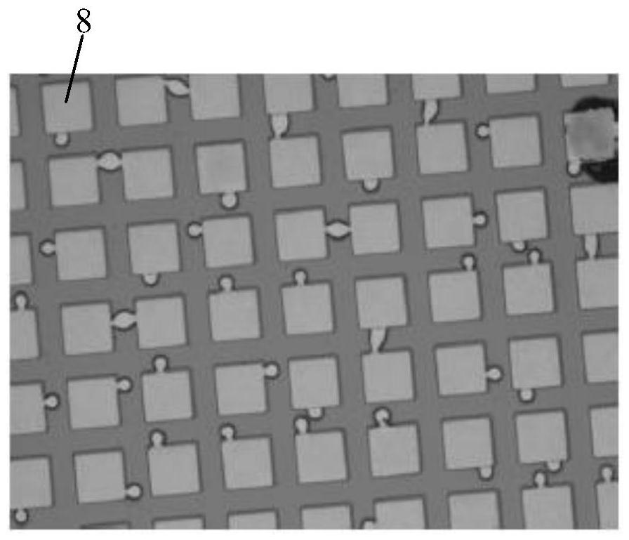
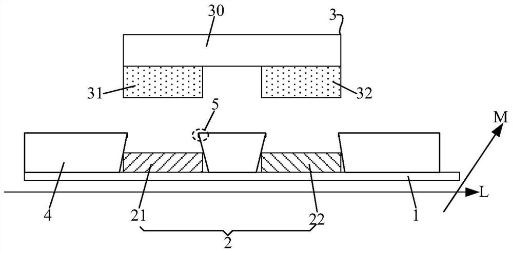
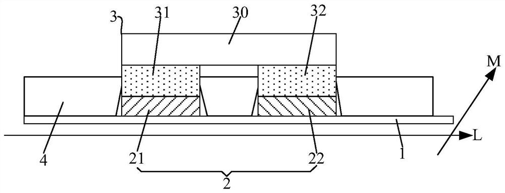
[0055] Currently, a eutectic bonding process is used to bond multiple micron-scale micro-LED chips to a backplane with transistor driver circuits. The traditional LED chip with horizontal electrodes has a large chip size and a large distance between the cathode and the anode. Using eutectic bonding and bonding will not cause the problem of short circuit caused by the liquefaction and flow of the electrode material, but the micro LED chip has a large chip size. Reduced to the micron level, and the distance between chips is close, in the process of using eutectic bonding, it is easy to cause the problem of short circuit between cathode and anode due to liquefaction flow of elec...


PUM


Abstract

The present invention provides a display substrate and a preparation method thereof. The display substrate includes a base, a plurality of binding electrodes and a plurality of functional elements, the binding electrodes are arranged on the base, the adjacent binding electrodes are spaced apart from each other, the functional elements are located on the side of the binding electrodes away from the base, and the binding electrodes are connected to The electrodes of the functional element are bound and connected, and a blocking structure is also arranged on the substrate, and the blocking structure is distributed at least in a part of the space area between the adjacent binding electrodes. The display substrate, by setting the blocking structure, can block the flow of the molten electrode material between the adjacent binding electrodes during eutectic bonding, so as to avoid the liquefaction flow of the electrode material and the adjacent binding electrodes. There is a problem of short circuit between the electrodes of the functional elements and between the electrodes of the functional elements; the blocking structure can clamp and fix the binding electrodes, thereby ensuring the firmness of the binding connection; there is also a certain warpage in the carrier plate carrying the functional elements. case to achieve good electrode binding.

Description

technical field [0001] The invention belongs to the field of display technology, and particularly relates to a display substrate and a preparation method thereof. Background technique [0002] Micro LED (Micro Light Emitting Diode, micro functional element) display technology, that is, LED miniaturization and matrix technology, refers to a high-density micro-sized LED array integrated on a chip, such as each pixel of the LED display can be found. It can be seen as a miniature version of the outdoor LED display, reducing the pixel distance from millimeters to micrometers. [0003] Current micro-LED mass transfer technology requires bonding multiple micron-scale LED chips to a backplane with transistor driver circuits. The traditional solution is to use conductive glue to bind the electrodes. The conductive glue contains conductive gold balls, and the conductive gold balls realize the bonding connection between the electrodes. However, for electrodes with a size of less than ...

Claims


Application Information

Patent Timeline
Patent Type & Authority Patents(China)
IPC IPC(8): H01L27/15
CPCH01L27/156H01L33/62H01L25/0753H01L25/167H01L2933/0066H01L24/95H01L24/81H01L2224/81193H01L2924/12041H01L2224/16257H01L24/16H01L24/13H01L2224/13013H01L2224/81001H01L2224/95001H01L2224/13166H01L2224/13109H01L2224/13124H01L2224/81399H01L2224/13155H01L2224/13147H01L2224/13111H01L2224/13144H01L2924/013H01L2924/00013H01L2924/00014H01L33/005H01L33/387H01L2933/0016
Inventor 陈右儒
Owner BOE TECH GRP CO LTD
Why Eureka
Try Eureka