Method for producing wafer by combining composite adhesive film with through hole glass carrier plate structure
A composite, glass technology, applied in the manufacture of electrical components, electric solid-state devices, semiconductor/solid-state devices, etc., can solve the problems of uniform coating layer, wafer damage, difficult to form, etc., to reduce production costs and avoid damage , the effect of improving production efficiency
- Summary
- Abstract
- Description
- Claims
- Application Information
AI Technical Summary
Problems solved by technology
Method used
Image
Examples
Embodiment 1
[0032] A method for producing a wafer with a composite adhesive film combined with a through-hole glass carrier structure, the method for producing the wafer includes the following steps:
[0033] S1: Holes on the glass carrier
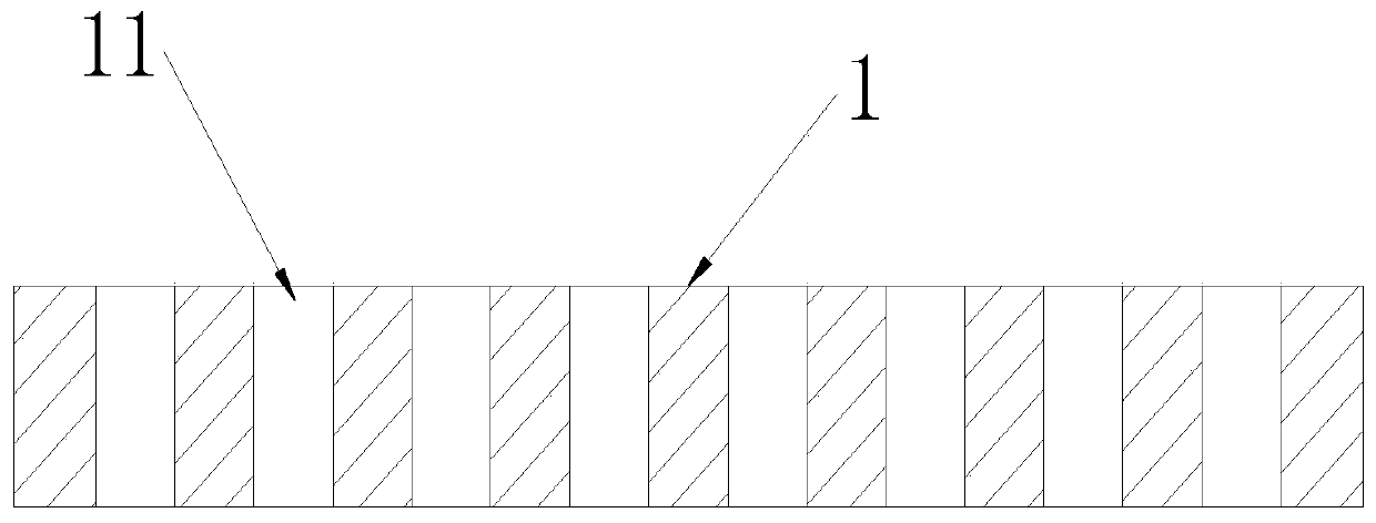
[0034] Through the yellow photomask pattern process, laser laser or etching process, the glass carrier 1 is opened with a pattern of window opening / TGV (via through glass carrier), and a glass window hole 11 is formed on the glass carrier 1, such as figure 1 shown.
[0035] S2: Wafer bonding on glass carrier
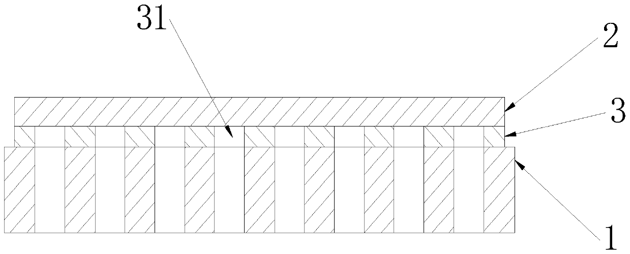
[0036] Paste the composite adhesive film 3 on the glass carrier 1, use an optical mechanism to accurately align the wafer 2 with the glass carrier 1, place the front of the wafer 2 on the composite adhesive film 3, and use the lamination pressure Bonding and heating the wafer 2 on the glass carrier 1, such as figure 2 shown.
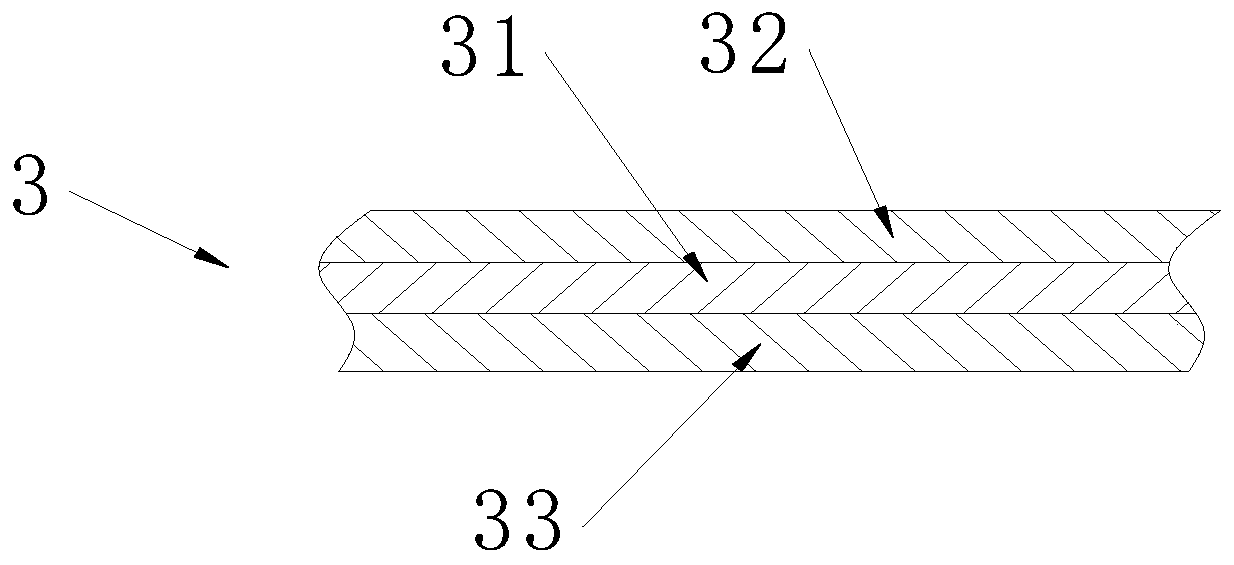
[0037] The composite adhesive film 3 includes a composite layer 32 , a heat treatment layer 31 and a UV light layer...
Embodiment 2
[0047] A method for producing a wafer with a composite adhesive film combined with a through-hole glass carrier structure, the method for producing the wafer includes the following steps:
[0048] S1: Holes on the glass carrier
[0049] Through the yellow photomask pattern process, laser laser or etching process, the glass carrier 1 is opened with a pattern of window opening / TGV (via through glass carrier), and a glass window hole 11 is formed on the glass carrier 1, such as figure 1 shown.
[0050] S2: Wafer bonding on glass carrier
[0051] Paste the composite adhesive film 3 on the glass carrier 1, use an optical mechanism to accurately align the wafer 2 with the glass carrier 1, place the front of the wafer 2 on the composite adhesive film 3, and use the lamination pressure Bonding and heating the wafer 2 on the glass carrier 1, such as figure 2 shown.
[0052] The composite adhesive film 3 includes a composite layer 32 , a heat treatment layer 31 and a UV light layer...
PUM
 Abstract
Description
Claims
Application Information
 - Generate Ideas
- Intellectual Property
- Life Sciences
- Materials
- Tech Scout
- Unparalleled Data Quality
- Higher Quality Content
- 60% Fewer Hallucinations
Browse by: Latest US Patents, China's latest patents, Technical Efficacy Thesaurus, Application Domain, Technology Topic, Popular Technical Reports.
© 2025 PatSnap. All rights reserved.Legal|Privacy policy|Modern Slavery Act Transparency Statement|Sitemap|About US| Contact US: help@patsnap.com


