Method for preparing dfb-ld grating debugging sample by electron beam exposure

A DFB-LD, electron beam exposure technology, applied in the field of microelectronics, can solve the problem of increasing the difficulty of observing the cross section of the electron beam DFB-LD grating, achieve the effect of reasonable exposure time, avoid pattern distortion, and improve the success rate

Active Publication Date: 2021-05-28
清华大学天津电子信息研究院
View PDF4 Cites 0 Cited by
  • Summary
  • Abstract
  • Description
  • Claims
  • Application Information

AI Technical Summary

Problems solved by technology

However, the width of 10-20μm is very difficult to be precisely cleaved, which greatly increases the difficulty of cross-sectional observation of the electron beam DFB-LD grating

Method used


Image

  • Method for preparing dfb-ld grating debugging sample by electron beam exposure
  • Method for preparing dfb-ld grating debugging sample by electron beam exposure
  • Method for preparing dfb-ld grating debugging sample by electron beam exposure

Examples


Embodiment Construction

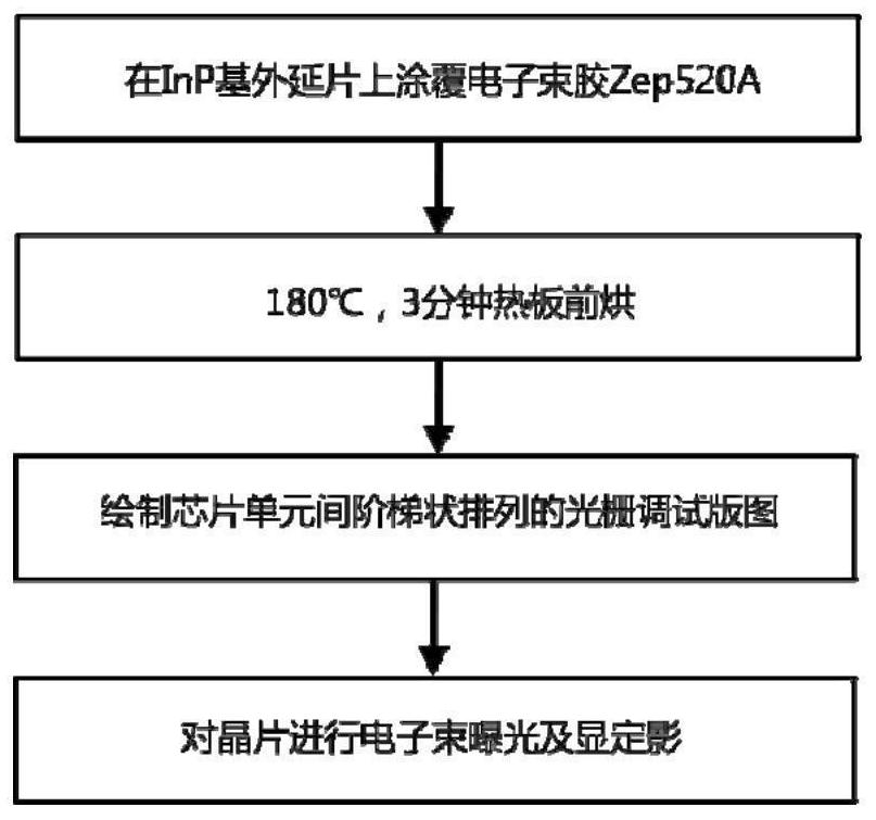
[0031] In order to further understand the invention content, characteristics and effects of the present invention, the following examples are given, and detailed descriptions are as follows in conjunction with the accompanying drawings:

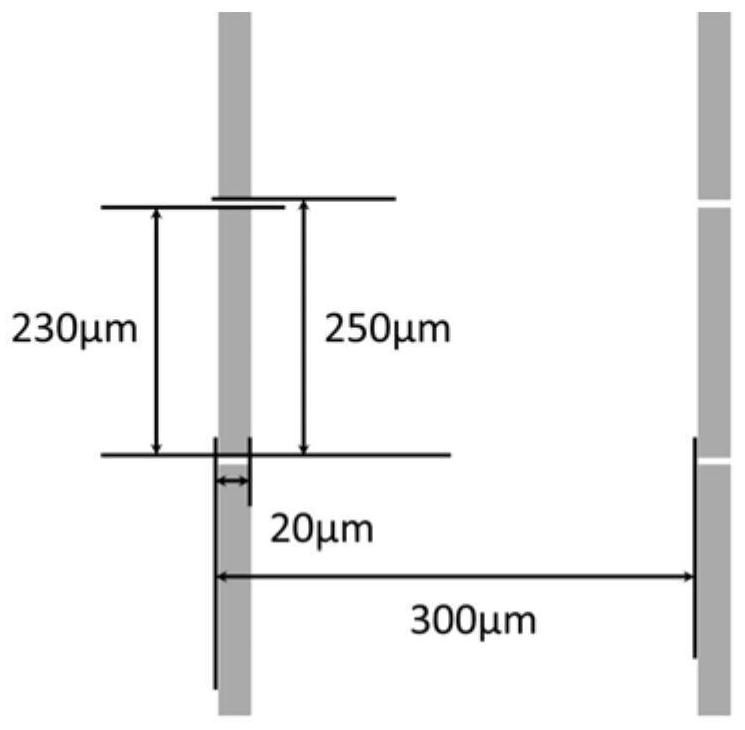
[0032] Such as Figure 1 to Figure 6 Shown, technical scheme of the present invention is:

[0033] A method for preparing DFB-LD grating debugging samples by electron beam exposure, which mainly optimizes the exposure layout according to the requirement of cross-section observation in the grating debugging process, which can greatly improve the efficiency of electron beam preparation of DFB-LD grating cross-section samples. Success rate. In this embodiment, an InP-based epitaxial wafer is taken as an example, and the method includes the following steps:

[0034] Step 1: Coat the electron beam gel Zep520A on the InP-based epitaxial wafer, the coating condition is 4000rpm, and the coating time is 40s;

[0035] Step 2: Put the InP-based epita...


PUM

PropertyMeasurementUnit
lengthaaaaaaaaaa
widthaaaaaaaaaa
lengthaaaaaaaaaa

Abstract

The invention discloses a method for preparing a DFB-LD grating debugging sample by electron beam exposure, which belongs to the field of microelectronics technology, comprising: step 1, coating electron beam glue on the wafer; step 2, pre-baking the wafer; 3. Use the layout design tool to draw the DFB‑LD grating debugging layout; based on the target DFB‑LD grating layout, under the premise of keeping the chip unit consistent with the target DFB‑LD grating layout, the DFB‑LD grating debugging layout is parallel to the grating direction The target DFB-LD grating layout is consistent, and the vertical grating direction changes from the grating alignment arrangement between the chip units to a stepped arrangement, and the staggered interval of the steps is equal to the length of the grating along the grating line; Fixing and hardening. By adopting the above technical solution, the present invention can improve the observation convenience and preparation success rate of grating section observation samples.

Description

technical field [0001] The invention belongs to the technical field of microelectronics, and in particular relates to a method for preparing a DFB-LD grating debugging sample by electron beam exposure. Background technique [0002] Since its invention in the 1960s, semiconductor lasers have developed rapidly due to their advantages of small size, high efficiency, low cost and high reliability. Adding a Bragg grating to the structure of an ordinary Fabry-Perot cavity semiconductor laser, through the diffraction effect of the grating, the laser can obtain a stable single longitudinal mode and significantly improve its beam quality. This laser is called Distributed feedback laser diode DFB-LD. [0003] DFB-LD grating preparation is very important in DFB-LD, and its preparation methods usually include two kinds of holographic exposure and electron beam exposure. Among these two methods, electron beam exposure can obtain high-quality grating mask patterns because electron beams...

Claims


Application Information

Patent Timeline
Patent Type & Authority Patents(China)
IPC IPC(8): G03F7/20H01S5/12
CPCG03F7/2063H01S5/12
Inventor 王岩曲迪黄翊东
Owner 清华大学天津电子信息研究院
Why Eureka
Try Eureka