Photosensitive detection unit based on composite dielectric gate structure, photosensitive detector and detection method

A composite medium and detection unit technology, applied to electrical components, electric solid devices, semiconductor devices, etc., can solve problems such as fixed pattern noise and device dark characteristic deterioration, achieve good dark characteristics, reduce dark noise, increase Quantity effect

Active Publication Date: 2020-08-18
NANJING UNIV
View PDF8 Cites 0 Cited by
  • Summary
  • Abstract
  • Description
  • Claims
  • Application Information

AI Technical Summary

Problems solved by technology

However, due to the presence of a depletion layer on the surface of the P-type substrate during the exposure process of the detector, the interface traps on the surface of the P-type substrate assisted to cause strong dark excitation, which would deteriorate the dark characteristics of the device, and the larger The dark signal of will bring more severe fixed pattern noise

Method used


Image

  • Photosensitive detection unit based on composite dielectric gate structure, photosensitive detector and detection method
  • Photosensitive detection unit based on composite dielectric gate structure, photosensitive detector and detection method
  • Photosensitive detection unit based on composite dielectric gate structure, photosensitive detector and detection method

Examples


Embodiment Construction

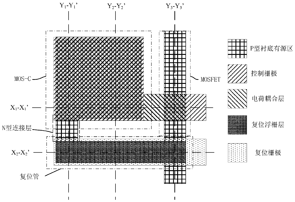
[0029] In this embodiment, the photosensitive detection unit pixel structure based on the compound dielectric gate structure is as follows: Figure 1-Figure 8As shown, each detector unit pixel includes a composite dielectric gate MOS-C part for light sensing, a composite dielectric gate MOSFET part for reading, and a reset tube part for reset. These three parts form On the same base P-type semiconductor material.

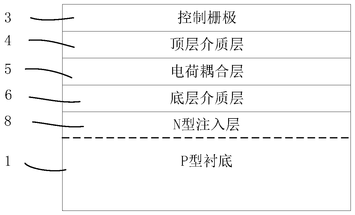
[0030] The structure of the composite dielectric gate MOS-C part used for photosensitive is as follows figure 2 As shown, it includes: a P-type semiconductor substrate 1; a bottom dielectric layer 6, a charge-coupled layer 5, a top dielectric layer 4, and a control gate 3 are arranged in sequence directly above the P-type semiconductor; Directly below) there may be an N-type implantation layer 8 formed by ion implantation doping, so as to move down the photo-charge storage position and leave the interface between the P-type semiconductor substrate and the top diel...


PUM


Abstract

The invention discloses a photosensitive detection unit based on a composite dielectric gate structure, a photosensitive detector and a detection method. The photosensitive detection unit comprises acomposite dielectric gate MOS-C part with a photosensitive function, a composite dielectric gate MOSFET part with an information reading function and a reset tube part with a reset function, wherein the reset tube part comprises a bottom dielectric layer, a reset floating gate layer, a top dielectric layer and a reset gate which are sequentially stacked above a P-type semiconductor substrate; in the P-type semiconductor substrate, an N-type connecting layer is arranged on the side close to a first bottom dielectric layer, and the N-type connecting layer is connected with an N-type injection layer; and the N-type injection layer is separated from an N-type source region, an N-type drain region, the substrate below the composite dielectric gate MOSFET part and the substrate below the reset gate by arranging a shallow trench isolation region and a P+ type injection region. According to the photosensitive detector, fixed pattern noise caused by dark signals is reduced, and the photosensitive detector has good dark characteristics and weak light response.

Description

technical field [0001] The present invention relates to imaging detection devices, especially the structure, working mechanism and signal readout of imaging detection devices from infrared, visible light to ultraviolet bands, and is a photosensitive detection unit with improved dark characteristics based on a composite dielectric grid structure, Detectors and methods for reading their signals. Background technique [0002] Imaging detectors are widely used in various fields such as military and civilian use. The main imaging detectors currently developed are CCD and CMOS-APS. CCD appeared earlier and its technology is relatively mature. Its basic structure is a series of MOS capacitors connected in series. The generation and change of potential wells on the surface of semiconductors are controlled by the voltage pulse sequence on the capacitors, and then the storage and transfer of photogenerated charge signals are realized. Due to this signal transfer feature, the charge t...

Claims


Application Information

Patent Timeline
Patent Type & Authority Applications(China)
IPC IPC(8): H01L27/146H01L29/423
CPCH01L27/14614H01L29/42364H01L29/42356H01L29/42324Y02P70/50
Inventor 闫锋王子豪沈凡翔李张南王凯胡心怡
Owner NANJING UNIV
Why Eureka
Try Eureka