based on mos 2 Homojunction field effect transistor and preparation method thereof

A field effect transistor and junction-type technology, which is applied in the field of MoS2-based homojunction junction field effect transistor and its preparation, can solve the problems of low carrier mobility and poor device performance, and achieve carrier migration The effect of high rate, large size and few defects

Active Publication Date: 2022-04-15
HUAZHONG UNIV OF SCI & TECH
View PDF4 Cites 0 Cited by
  • Summary
  • Abstract
  • Description
  • Claims
  • Application Information

AI Technical Summary

Problems solved by technology

[0005] The present invention provides a MoS-based 2 The homojunction junction field effect transistor and its preparation method, to solve the problem of low carrier mobility and poor device performance

Method used


Image

  • based on mos  <sub>2</sub> Homojunction field effect transistor and preparation method thereof
  • based on mos  <sub>2</sub> Homojunction field effect transistor and preparation method thereof
  • based on mos  <sub>2</sub> Homojunction field effect transistor and preparation method thereof

Examples


preparation example Construction

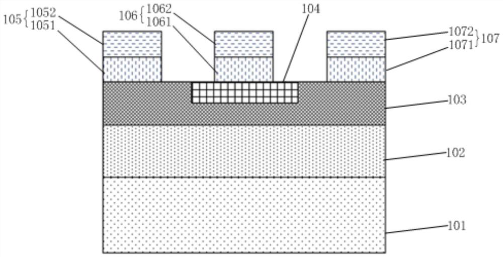
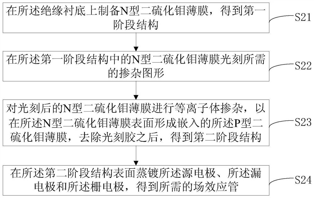
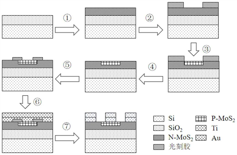
[0060] Please refer to figure 2 and image 3 , for the MoS-based 2 A homojunction field effect transistor, this embodiment also provides a preparation method, including:

[0061] S21: preparing an N-type molybdenum disulfide film on the silicon substrate to obtain a first-stage structure;

[0062] S22: Doping patterns required for photolithography of N-type molybdenum disulfide thin films in the first-stage structure;

[0063] S23: Perform plasma doping on the N-type molybdenum disulfide thin film after photolithography, so as to form the embedded P-type molybdenum disulfide thin film on the surface of the N-type molybdenum disulfide thin film, and after removing the photoresist, obtain the first two-stage structure;

[0064] S24: Evaporating the source electrode, the drain electrode, and the gate electrode on the surface of the second-stage structure to obtain a desired field effect transistor.

[0065] In one of the implementation manners, step S21 may include:

[006...


PUM

PropertyMeasurementUnit
thicknessaaaaaaaaaa
thicknessaaaaaaaaaa
thicknessaaaaaaaaaa

Abstract

The present invention provides a MoS-based 2 Homojunction junction field effect transistor and preparation method thereof, wherein the MoS-based 2 The homojunction junction field effect transistor includes: a silicon substrate, an N-type molybdenum disulfide film, a P-type molybdenum disulfide film, a source electrode, a drain electrode and a gate electrode; the N-type molybdenum disulfide film is provided in the On one side of the silicon substrate, the P-type molybdenum disulfide film is embedded in the surface of the N-type molybdenum disulfide film on the side opposite to the silicon substrate; the gate electrode is arranged on the P-type The side surface of the molybdenum disulfide thin film facing away from the silicon substrate, the source electrode and the drain electrode are provided on the side surface of the N-type molybdenum disulfide thin film facing away from the silicon substrate , and the gate electrode is located between the source electrode and the drain electrode.

Description

technical field [0001] The invention relates to the field of semiconductors, in particular to a MoS-based 2 A homojunction field effect transistor and a preparation method thereof. Background technique [0002] Two-dimensional transition metal dichalcogenides (TMDs) have attracted much attention due to their extremely high electron mobility and other excellent optical, electrical, mechanical, chemical, acoustic, mechanical and other properties. The structure of transition metal chalcogenides is similar, and the semiconductor properties are also similar, for example, the band gap changes with the number of layers. in MoS 2 For example, MoS 2 It is a typical two-dimensional transition metal chalcogenide whose bandgap (1.2eV-1.8eV) changes with the number of layers. MoS2 has a high carrier mobility, and the single-layer carrier mobility can reach 410cm 2 V -1 the s -1 , multilayer carrier mobility up to 500cm 2 V -1 the s -1 . Due to the many excellent properties of ...

Claims


Application Information

Patent Timeline
Patent Type & Authority Patents(China)
IPC IPC(8): H01L29/808H01L29/06H01L21/336H01L29/10H01L29/24
CPCH01L29/8083H01L29/0603H01L29/0684H01L29/66901H01L29/1033H01L29/24
Inventor 曾祥斌鲁基昌王文照陆晶晶王士博胡一说肖永红王君豪周宇飞袁俊茹王曦雅
Owner HUAZHONG UNIV OF SCI & TECH
Why Eureka
Try Eureka