Ultra-wideband spiral laminated wave absorber
A spiral, ultra-broadband technology, applied in the direction of instruments, optics, electrical components, etc., can solve the problems of limited application, low performance, high density, etc., and achieve the effects of diverse functions, reduced reflection and scattering, and flexible design
- Summary
- Abstract
- Description
- Claims
- Application Information
AI Technical Summary
Problems solved by technology
Method used
Image
Examples
Embodiment 1
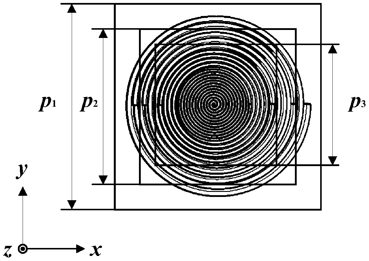
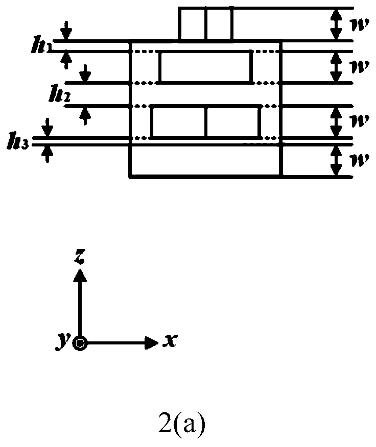
[0033] Embodiment one, as image 3 As shown in (a), an ultra-broadband spiral laminated absorber includes: a metal reflective layer is arranged on the bottom layer, and an ultra-wideband spiral laminated absorber is arranged on the metal reflective layer. In this embodiment, the ultra-wideband spiral laminated absorber The unit includes a layer of dielectric layer, the top layer of Archimedes spiral metal structure is set on the dielectric layer, and two layers of Archimedes spiral metal structure are embedded in the medium layer; all Archimedes spiral metal structures can be moved from the bottom layer to the The top layer is divided into a pyramid structure with the same number as the medium layer. The side view of this embodiment is as figure 2 As shown in (a), where optionally, the distance between the bottom metal reflector and the first layer of Archimedes spiral from bottom to top h 3 =20 nm, the distance between the first layer of Archimedes spiral and the second l...
Embodiment 2
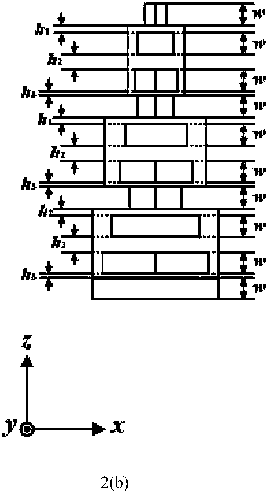
[0034] Embodiment two, such as image 3 As shown in (b), an ultra-wideband spiral laminated absorber includes: a metal reflective layer is arranged on the bottom layer, and an ultra-wideband spiral laminated absorber is arranged on the metal reflective layer. In this embodiment, the ultra-wideband spiral laminated absorber The wave unit includes a first dielectric layer, a second dielectric layer and a third dielectric layer arranged from the bottom layer to the top layer, the first dielectric layer is arranged on the metal reflective layer, and the absorber has a total of nine layers from bottom to top. The Mead spiral metal structure includes two layers of Archimedes spiral metal structures embedded in the first dielectric layer starting from the bottom layer, and a layer of Archimedes spiral metal structures is arranged between the first dielectric layer and the second dielectric layer, and The two-layer Archimedes spiral metal structure embedded in the first medium layer a...
Embodiment 3
[0038] Embodiment 3. An ultra-broadband helical laminated wave absorber. The three-dimensional view of the embodiment is as follows image 3 As shown in (c), the side view is as figure 2 As shown in (c), this embodiment includes a metal reflective layer arranged on the bottom layer, and an ultra-broadband spiral laminated absorbing unit is arranged on the metal reflective layer. In this embodiment, the ultra-wideband spiral laminated absorber, such as image 3 (c) and figure 2 As shown in (c), the unit structure of the ultra-broadband spiral laminated absorbing unit includes a pyramid-shaped medium composed of the first dielectric layer 12, the second dielectric layer 11 and the third dielectric layer 10, and the first dielectric layer 12 set on the metal reflective layer 13. The first to nine layers of spiral resonance structures 1, 2, 3, 4, 5, 6, 7, 8, 9 (that is, the Archimedes spiral resonance structure, hereinafter referred to as the spiral structure or Archimedes spi...
PUM
| Property | Measurement | Unit |
|---|---|---|
| Radius | aaaaa | aaaaa |
| Thickness | aaaaa | aaaaa |
| Side length | aaaaa | aaaaa |
Abstract
Description
Claims
Application Information
 - Generate Ideas
- Intellectual Property
- Life Sciences
- Materials
- Tech Scout
- Unparalleled Data Quality
- Higher Quality Content
- 60% Fewer Hallucinations
Browse by: Latest US Patents, China's latest patents, Technical Efficacy Thesaurus, Application Domain, Technology Topic, Popular Technical Reports.
© 2025 PatSnap. All rights reserved.Legal|Privacy policy|Modern Slavery Act Transparency Statement|Sitemap|About US| Contact US: help@patsnap.com


