


Quick Research
Generate reliable direction feasibility study reports for your R&D in just a few steps.

Technical Q&A
Discover and master advanced knowledge NOW. Basics, ideas, possibilities, all at once.

Find Solutions
As an expert in R&D theories, this can generate solutions to your technical problems instantly.

Evaluate Feasibility
Analyze your overall solution with one click, know your potential R&D risks in advance.

Monitor Landscape
Get weekly tech updates, stay abreast of the latest tech innovations and key insights.
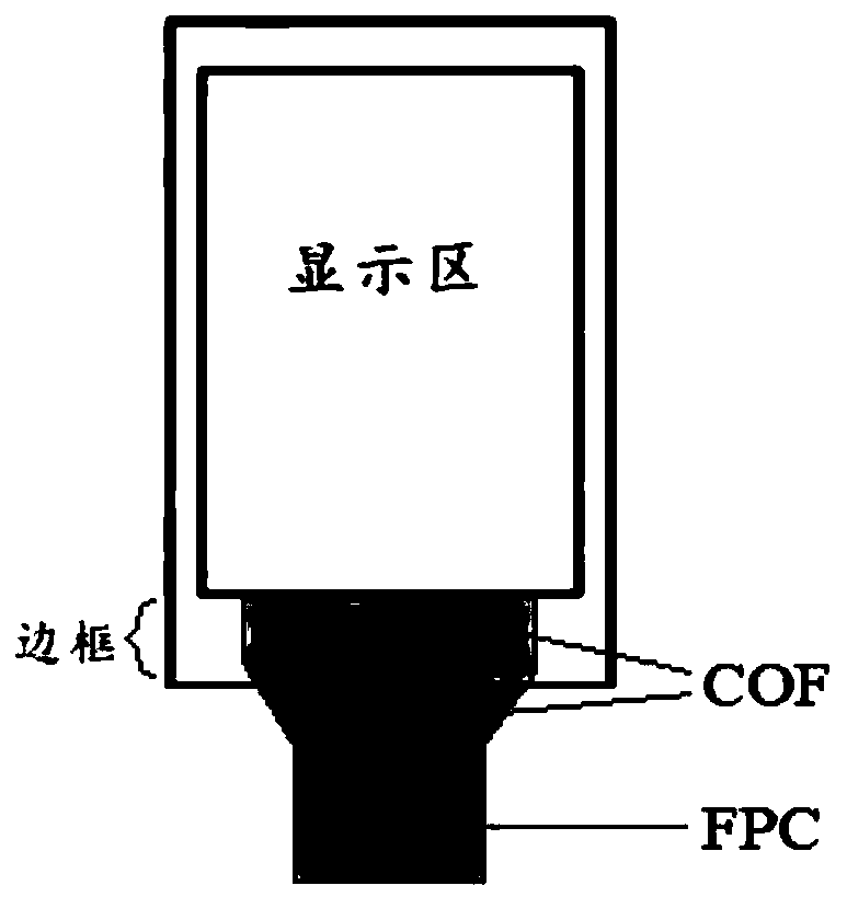
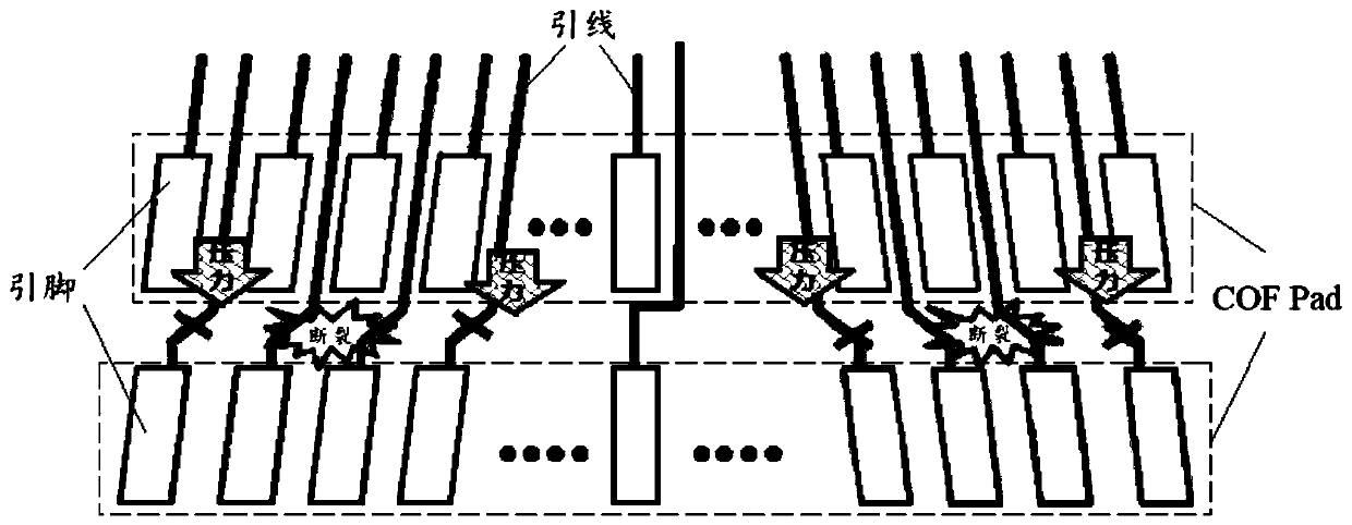
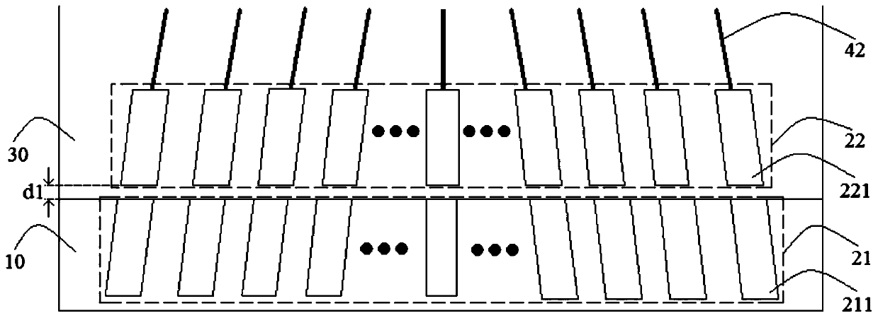
Display device and manufacturing method thereof
A technology for a display device and a manufacturing method, which is applied to identification devices, semiconductor/solid-state device manufacturing, static indicators, etc., can solve the problems of complex wiring, large number of pixels on large-size screens, etc., to ensure stability and improve binding. The effect of a display device with a fixed yield and a narrow bezel
- Summary
- Abstract
- Description
- Claims
- Application Information
AI Technical Summary
Problems solved by technology
Method used
Image

Examples
Embodiment Construction
[0048] In order to make the object, technical solution and advantages of the present invention clearer, the present invention will be described in further detail below in conjunction with specific embodiments and with reference to the accompanying drawings.
[0049]It should be noted that, unless otherwise defined, the technical terms or scientific terms used in the embodiments of the present invention shall have the usual meanings understood by those skilled in the art to which the present disclosure belongs. "First", "second" and similar words used in the present disclosure do not indicate any order, quantity or importance, but are only used to distinguish different components. "Comprising" or "comprising" and similar words mean that the elements or items appearing before the word include the elements or items listed after the word and their equivalents, without excluding other elements or items. Words such as "connected" or "connected" are not limited to physical or mechani...
PUM
 Abstract
Description
Claims
Application Information
 - R&D Engineer
- R&D Manager
- IP Professional
- Industry Leading Data Capabilities
- Powerful AI technology
- Patent DNA Extraction
Browse by: Latest US Patents, China's latest patents, Technical Efficacy Thesaurus, Application Domain, Technology Topic, Popular Technical Reports.
© 2024 PatSnap. All rights reserved.Legal|Privacy policy|Modern Slavery Act Transparency Statement|Sitemap|About US| Contact US: help@patsnap.com