Manufacturing method of shield gate trench power device

A technology of power devices and manufacturing methods, which is applied in the manufacture of semiconductor/solid-state devices, semiconductor devices, electrical components, etc., can solve problems such as electrical failure, abnormal morphology of polysilicon etching back, and damage to charge balance, so as to improve the appearance, Improve device performance, improve the effect of device electrical properties

Active Publication Date: 2020-07-10
GUANGZHOU CANSEMI TECH INC
View PDF6 Cites 1 Cited by
  • Summary
  • Abstract
  • Description
  • Claims
  • Application Information

AI Technical Summary

Problems solved by technology

Due to the characteristics of the CVD process, the width at the top of the trench is often smaller than the width at the middle and bottom, forming a "closed" shape of the trench, which will cause voids to be formed in the middle or bottom of the trench when polysilicon is filled ( void), eventually resulting in abnormal morphology of polysilicon when it is etched back, destroying the charge balance, leading to final electrical failure

Method used


Image

  • Manufacturing method of shield gate trench power device
  • Manufacturing method of shield gate trench power device
  • Manufacturing method of shield gate trench power device

Examples


Embodiment Construction

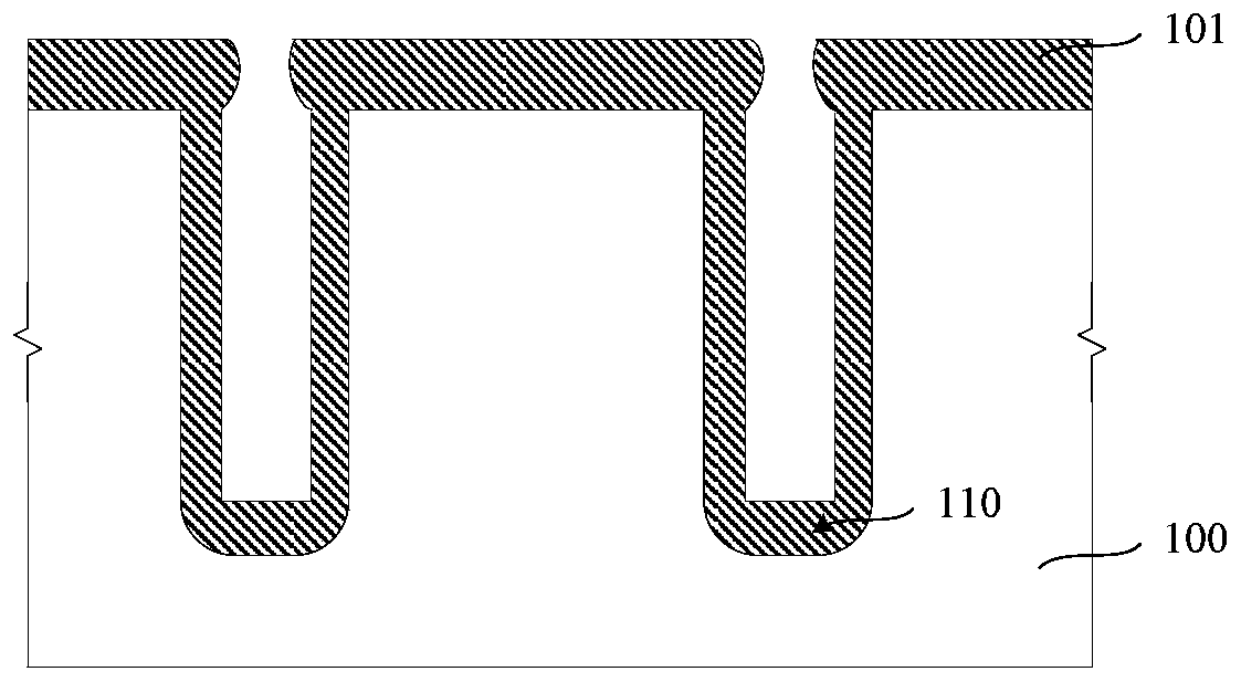
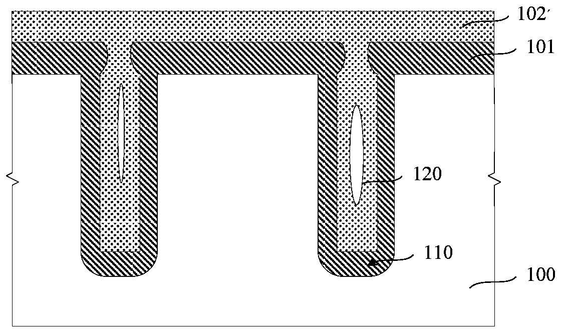
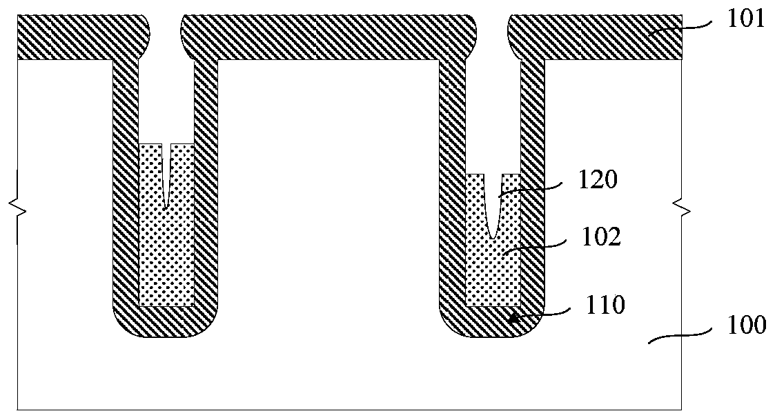
[0035] Figure 1A to Figure 1C It is a structural schematic diagram corresponding to corresponding steps of a manufacturing method of a shielded gate trench power device.

[0036] First, refer to Figure 1A As shown, a trench 110 is formed on a substrate 100 , a dielectric layer 101 is formed at the bottom and sidewalls of the trench 110 , and the dielectric layer 102 extends to cover the surface of the substrate 100 . The dielectric layer 101 is formed in two steps of a thermal oxidation method and a CVD process. Due to the characteristics of the CVD process, the dielectric layer on the surface of the substrate 100 extends toward the center of the trench 110, so that the width of the top of the trench 110 is smaller than that in the middle. and the width of the bottom form the “closed” shape of the trench 110 .

[0037] Next, refer to Figure 1B As shown, the trench 110 is filled with a shielding gate material layer 102 ′, and the shielding gate material layer 102 ′ extends...


PUM

PropertyMeasurementUnit
thicknessaaaaaaaaaa

Abstract

The invention provides a manufacturing method of a shield gate trench power device, which comprises the following steps: providing a substrate with trenches, forming dielectric layers at the bottoms and on the side walls of the trenches, and extending the dielectric layers to the surface of the substrate; filling the trenches with sacrificial layers, wherein the sacrificial layers extend to coverthe dielectric layers on the surface of the substrate; removing the sacrificial layers; and filling the trenches with shielding gate material layers. Before the trenches are filled with the shieldinggate material layers, the trenches are filled with the sacrificial layers, and the closing openings in the top ends of the trenches are weakened or eliminated by etching the sacrificial layers, so that cavities are prevented from occurring in the filling process of the shielding gate material layers, and the electrical property of the device is improved. Further, the sacrificial layers are removedin two steps, after the sacrificial layers are etched to a first preset height position of the trenches in the first step, the exposed dielectric layers are cleaned by a wet method, and under the condition of not influencing the morphology of the lower parts of the trenches, the inclination angles of the openings in the top ends of the trenches are increased, the morphology of the upper parts ofthe trenches is improved, the filling capability of the shielding gate material layers is improved, the cellular density is improved and the device performance is improved.

Description

technical field [0001] The invention relates to the field of integrated circuit manufacturing, in particular to a method for manufacturing shielded gate trench power devices. Background technique [0002] Since the invention of power MOS technology, the technology has achieved many important developments and great progress. In recent years, new device structures and new manufacturing processes of power MOS technology have emerged continuously to achieve two basic goals: maximum power handling capability and minimum power loss. Trench MOSFET (Trench MOS) technology is one of the most important technological driving forces to achieve this goal. Initially, Trench MOS technology was invented to increase the channel density of planar devices to improve the current handling capability of the device, but its channel density and drift region resistance are not yet ideal. [0003] Therefore, the industry has further proposed a new Trench MOS structure. The new Trench MOS structure ...

Claims


Application Information

Patent Timeline
Patent Type & Authority Applications(China)
IPC IPC(8): H01L21/336H01L21/28
CPCH01L29/66734H01L21/28035
Inventor 宁润涛黄康荣
Owner GUANGZHOU CANSEMI TECH INC
Why Eureka
Try Eureka