A semiconductor testing equipment

A test equipment and semiconductor technology, used in high-speed test scenarios without signal attenuation, semiconductor test equipment, can solve problems such as heat dissipation to be improved, high frequency energy attenuation, inability to solve applications, etc., to prevent power supply and signal board damage, high The effect of low frequency energy attenuation and preventing equipment damage

Active Publication Date: 2022-02-18
武汉精鸿电子技术有限公司
View PDF8 Cites 0 Cited by
  • Summary
  • Abstract
  • Description
  • Claims
  • Application Information

AI Technical Summary

Problems solved by technology

[0004] However, this solution cannot solve the application of some specific scenarios, such as the test for high-speed bus (> 1Gbps+), separate test equipment and the unit under test, there is a problem of excessive high-frequency energy attenuation, and the heat dissipation needs to be improved

Method used


Image

  • A semiconductor testing equipment
  • A semiconductor testing equipment
  • A semiconductor testing equipment

Examples


Embodiment Construction

[0045] In order to make the object, technical solution and advantages of the present invention clearer, the present invention will be further described in detail below in conjunction with the accompanying drawings and embodiments. It should be understood that the specific embodiments described here are only used to explain the present invention, not to limit the present invention. In addition, the technical features involved in the various embodiments of the present invention described below can be combined with each other as long as they do not constitute a conflict with each other. The present invention will be further described in detail below in combination with specific embodiments.

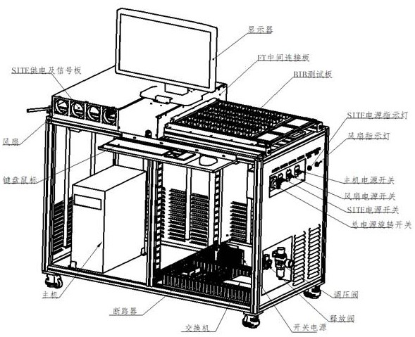
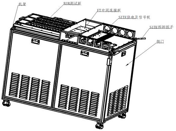
[0046] As a preferred embodiment of the present invention, such as Figure 1-2As shown, the present invention provides a semiconductor testing device, which includes an electronic control module, a testing module, an air source circuit, a cooling module, and a display module arranged on a f...


PUM


Abstract

The invention relates to the field of semiconductor testing, and discloses a semiconductor testing device, which is characterized in that it includes an electric control module, a test module, an air source circuit, and a heat dissipation module arranged on a rack; the test module includes a BIB test board and a SITE The power supply and signal board, the BIB test board and the SITE power supply and signal board are respectively hard-docked with the FT intermediate connection board wireless material; the front of the BIB test board is provided with a device to be tested, and the back of the BIB test board is connected with The test core board, the air source circuit is set facing the test core board, and the heat dissipation module is set right facing the BIB test board for cooling the BIB test board. The invention provides a complete set of testing equipment for high-speed DUTs, realizes high-speed bus testing, and solves the problem of device heat dissipation in the testing process.

Description

technical field [0001] The invention belongs to the field of semiconductor testing, especially for high-speed testing without signal attenuation, and specifically relates to semiconductor testing equipment. Background technique [0002] With the rapid development of semiconductor manufacturing technology, high-speed and high-capacity memories emerge in an endless stream, and the demand for semiconductor memory test equipment is also increasing. [0003] The existing solutions are to separate the test system from the device under test (DUT), place the DUT in a thermostat that supports a wide range of ambient temperatures, and place the test system in a normal temperature environment. The test system and DUT are connected through PCB and connectors. [0004] However, this solution cannot solve the application of some specific scenarios, such as the test for high-speed bus (> 1Gbps+), separate test equipment and the unit under test, there is a problem of excessive high-freq...

Claims


Application Information

Patent Timeline
Patent Type & Authority Patents(China)
IPC IPC(8): G01R31/26
CPCG01R31/2601
Inventor 曹锐邓标华裴敬杜建
Owner 武汉精鸿电子技术有限公司
Why Eureka
Try Eureka