
High-speed and high-linearity grid voltage bootstrap switching circuit

A gate voltage bootstrap, switching circuit technology, applied in electronic switches, electrical components, pulse technology and other directions, can solve problems such as affecting the overall speed of the circuit, ignoring nonlinear problems, affecting the linearity of the circuit, etc., to reduce the body effect, The effect of reducing the number of tubes and improving the linearity

Active Publication Date: 2020-06-05
UNIV OF ELECTRONICS SCI & TECH OF CHINA
View PDF10 Cites 6 Cited by
  • Summary
  • Abstract
  • Description
  • Claims
  • Application Information

AI Technical Summary

Problems solved by technology

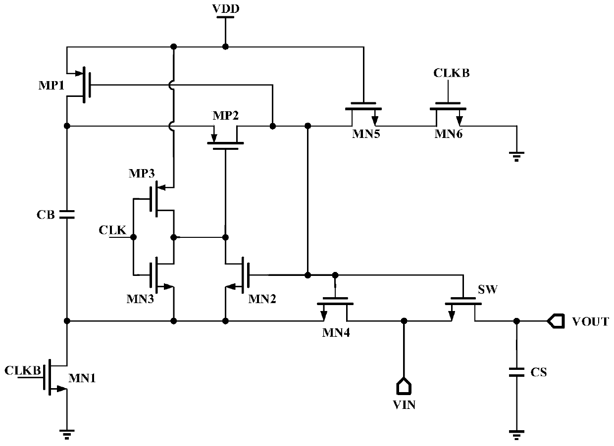
[0009] By using the gate voltage bootstrap switch circuit, the gate-source voltage V of the sampling switch tube is reduced GS The nonlinear distortion caused by the change, but it ignores the sampling switch conduction threshold voltage V caused by the body effect TH0 Non-linear problems brought about by the changes, and there are also challenges in the application of high-speed ADCs
This is because the traditional gate voltage bootstrap switch has a large parasitic capacitance because the gate terminal of the sampling switch SW is connected to multiple MOS transistors, which causes the gate voltage of SW to decrease compared with the ideal value, and at the same time Affect the overall speed of the circuit; and the body effect of the switch tube SW will affect the linearity of the circuit

Method used


Image

  • High-speed and high-linearity grid voltage bootstrap switching circuit
  • High-speed and high-linearity grid voltage bootstrap switching circuit

Examples


Embodiment Construction

[0026] The present invention will be described in detail below in conjunction with the accompanying drawings and specific examples.

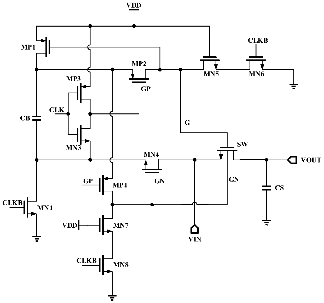
[0027] The present invention proposes a high-speed and high-linearity gate voltage bootstrap switch circuit, such as figure 2 As shown, it includes the first capacitor CB, the first NMOS transistor MN1, the third NMOS transistor MN3, the fourth NMOS transistor MN4, the fifth NMOS transistor MN5, the sixth NMOS transistor MN6, the seventh NMOS transistor MN7, the eighth NMOS transistor, The first PMOS transistor MP1, the second PMOS transistor MP2, the third PMOS transistor MP3, the fourth PMOS transistor MP4 and the sampling switch SW, the gate of the first PMOS transistor MP1 is connected to the drain of the fifth NMOS transistor MN5, the second PMOS The drain of the tube MP2 and the gate of the sampling switching tube SW, its source is connected to the source of the third PMOS transistor MP3 and the gate of the fifth NMOS transistor MN5 and c...


PUM


Abstract

The invention, which belongs to the technical field of analog circuit, discloses a high-speed and high-linearity grid voltage bootstrap switching circuit. According to the invention, GN node signals generated by a fourth PMOS transistor, an eighth NMOS transistor and a seventh NMOS transistor are used for controlling the grid electrode of the fourth NMOS transistor; in addition, the same signal, namely a GN node signal, is used for controlling a substrate of a sampling switch tube, so that the substrate potential of the sampling switch tube is kept consistent with the grid potential during sampling, and thus the speed of the circuit is increased; the parasitic capacitance of the grid terminal of the sampling switch tube is reduced by reducing the number of the tubes connected with the gridterminal of the sampling switch tube; meanwhile, the bulk effect in the secondary effect of the MOS tube is reduced, the linearity of the sampling switch tube is ensured, and finally, the precisionof the sampling switch circuit is improved.

Description

technical field [0001] The invention belongs to the technical field of analog integrated circuits, and in particular relates to a high-speed and high-linearity gate voltage bootstrap switch circuit, which can be used in a sample-and-hold circuit. Background technique [0002] With the advancement of integrated circuit technology and the rapid growth of communication and multimedia markets, digital signal processing technology has also been rapidly developed and widely used in various fields. Digital signals have the advantages of strong anti-interference ability, easy integration, low power consumption, and low cost. Therefore, more and more analog signal processing is gradually replaced by digital signal technology. However, light, heat, sound, electricity, magnetism and other signals in nature are all analog quantities. In order to make these analog signals be processed by digital systems, it is necessary to convert these time-continuous analog signals into discrete digita...

Claims


Application Information

Patent Timeline
Patent Type & Authority Applications(China)
IPC IPC(8): H03K17/687
CPCH03K17/687Y02B70/10
Inventor 唐鹤张浩松韦祖迎彭析竹
Owner UNIV OF ELECTRONICS SCI & TECH OF CHINA
Learn More