Graphene homogeneous p-n junction structure and preparation method thereof

A technology of graphene and graphene layers, applied in semiconductor/solid-state device manufacturing, electrical components, circuits, etc., can solve problems such as different chemical properties, performance parameter differences, doping effects, etc., to reduce dislocations and defects, improve performance Excellent, structurally stable effect

Pending Publication Date: 2020-06-05
XI'AN PETROLEUM UNIVERSITY
View PDF3 Cites 1 Cited by
  • Summary
  • Abstract
  • Description
  • Claims
  • Application Information

AI Technical Summary

Problems solved by technology

However, the p-n junction heterostructure composed of graphene and semiconductor materials will cause interface problems, which will affect the performance of microelectronic devices.
[0004] Although graphene itself exhibits excellent intrinsic properties, due to the influence of the substrate during preparation, the performance parameters obtained when doped with graphene are still quite different from the theoretical calculations.
In the process of preparing graphene by micromachining, it is necessary to transfer the prepared graphene to different substrates, but due to the different chemical properties of the two, a certain amount of charge transfer will occur, which will eventually cause doping effects and interface problems.

Method used


Image

  • Graphene homogeneous p-n junction structure and preparation method thereof
  • Graphene homogeneous p-n junction structure and preparation method thereof
  • Graphene homogeneous p-n junction structure and preparation method thereof

Examples


preparation example Construction

[0039] The preparation method of graphene homogeneous p-n junction structure of the present invention comprises following process:

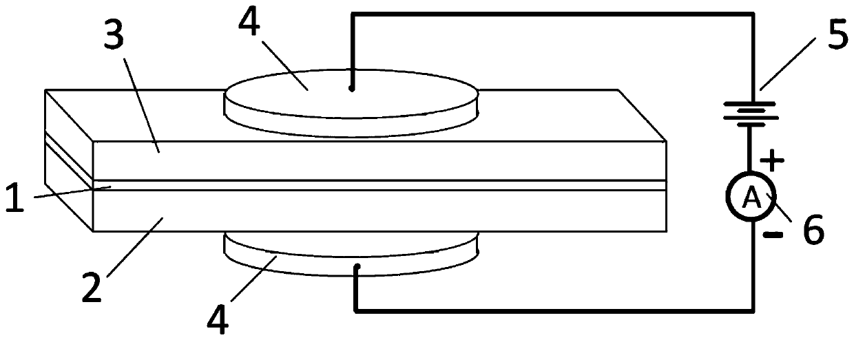
[0040] Prepare p-type graphene layer 2 / neutral graphene layer 1 / n-type graphene layer 3 composite structure;

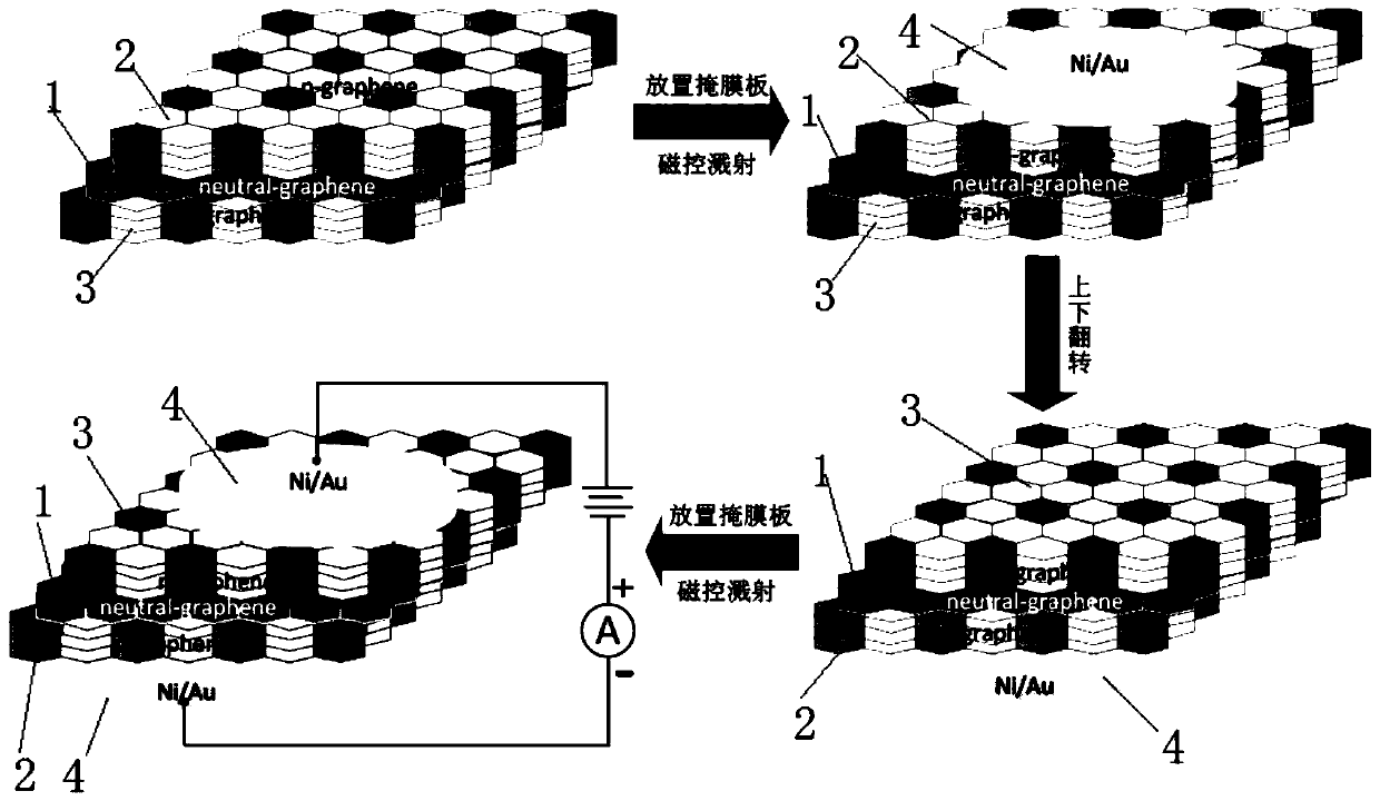
[0041] Electrodes 4 are prepared on the surface of the p-type graphene layer 2 and the surface of the n-type graphene layer 3 to obtain the graphene homogeneous p-n junction structure.

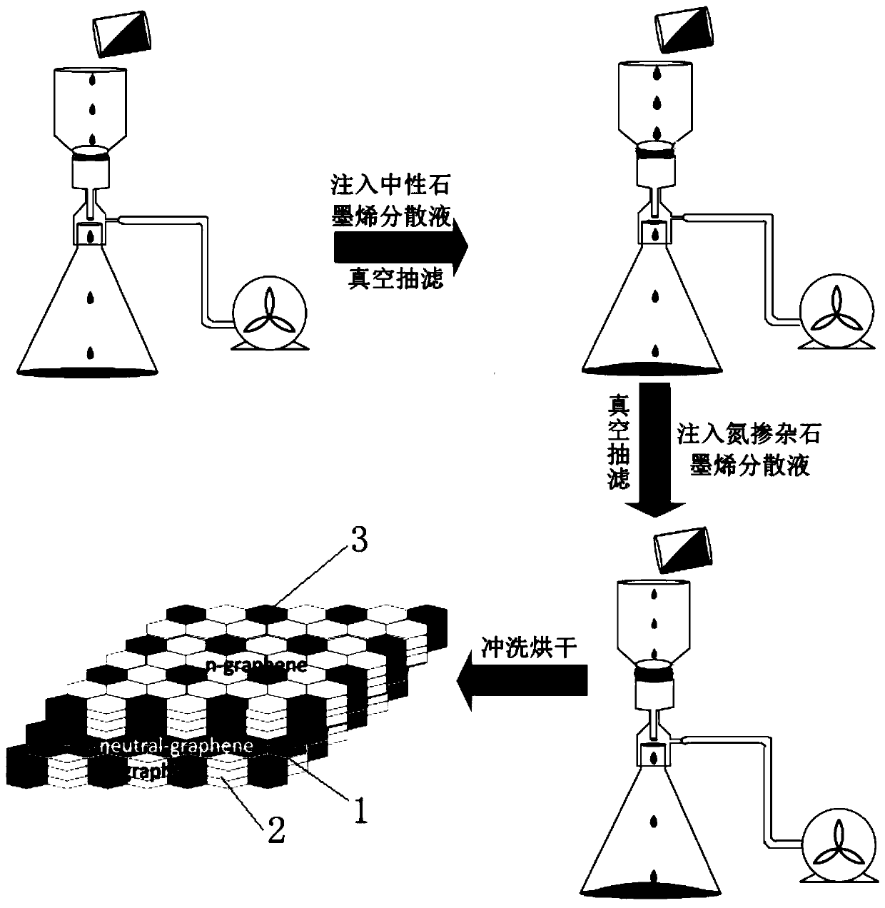
[0042] As a preferred embodiment of the present invention, the homogeneous p-n junction graphene-based paper of p-type graphene layer / neutral graphene layer / n-type graphene layer is prepared by vacuum filtration method, and then the homogeneous p-n junction graphene-based paper The paper is cleaned and dried to obtain a composite structure of p-type graphene layer / neutral graphene layer / n-type graphene layer, and the electrode 4 is prepared by magnetron sputtering.

[0043] As a preferred embodiment of the present invention, the neutral graphene layer 1...

Embodiment

[0045] In this example, the compound of graphene oxide and doped target atoms (boron, nitrogen) is used as raw materials, and the traditional vacuum filtration technology is used to prepare the graphene homogeneous p-n junction structure at one time, and the same material has thermal expansion coefficient, electronic The affinity energy, band gap width and lattice constant are all the same, which avoids the problem of interface characteristics caused by the heterojunction formed by different materials.

[0046] This embodiment adopts the following technical solutions to achieve:

[0047] 1. Preparation of boron-doped graphene and nitrogen-doped graphene;

[0048] 2. Prepare graphene homogeneous p-n junction by traditional vacuum filtration technology;

[0049] 3. Preparation of Ni / Au circular electrodes by magnetron sputtering.

[0050] Here are the detailed steps for each step:

[0051] 1. Preparation of boron-doped graphene and nitrogen-doped graphene

[0052] Graphene o...


PUM

PropertyMeasurementUnit
Thicknessaaaaaaaaaa
Thicknessaaaaaaaaaa
Diameteraaaaaaaaaa

Abstract

The invention discloses a graphene homogeneous p-n junction structure and a preparation method thereof. The graphene homogeneous p-n junction structure comprises a neutral graphene layer, a p-type graphene layer, an n-type graphene layer and an electrode, wherein the p-type graphene layer is arranged on the surface of one side of the neutral graphene layer, the n-type graphene layer is arranged onthe surface of the other side of the neutral graphene layer, and electrodes are arranged on the surface of the p-type graphene layer and the surface of the n-type graphene layer. According to the invention, the characteristics of the same material of graphene that the thermal expansion coefficient, the electron affinity, the band gap width and the lattice constant are the same are utilized; therefore, the complex interface problem generated by heterogeneous p-n junctions made of different materials and the problems of structural instability, low efficiency and the like of the heterogeneous p-n junctions are avoided, and meanwhile, the p-n junction structure has excellent flexibility and performance and can be used for structural design of flexible electronic devices and research and development of a high-performance miniaturized fine display technology.

Description

technical field [0001] The invention belongs to the technical field of microelectronic devices, and in particular relates to a graphene homogeneous p-n junction structure and a preparation method thereof. Background technique [0002] With the continuous improvement of the operating speed and performance requirements of microelectronic devices in various fields, new high-performance functional devices based on two-dimensional semiconductor materials have attracted more and more attention. The rapid response of microelectronic devices has become an important link and key direction to break through the current technical bottleneck. The most representative solid-state semiconductor device is the transistor, which acts as a variable switch. Transistors currently being researched or used are broadly classified into three categories: silicon-based thin film transistors, oxide thin film transistors, and organic thin film transistors. After years of development, the silicon-based ...

Claims


Application Information

Patent Timeline
IPC IPC(8): H01L29/16H01L29/861H01L29/868H01L21/329
CPCH01L29/1606H01L29/868H01L29/8613H01L29/6603
Inventor 丁继军靳岩鑫陈海霞傅海威屈永锋李辉栋
Owner XI'AN PETROLEUM UNIVERSITY
Why Eureka
Try Eureka