Compound, composition for encapsulating photoelectric device, preparation method, encapsulation film, electronic device, and encapsulation method
A technology for optoelectronic devices and encapsulation films, which is applied in the fields of compounds, compositions for optoelectronic device encapsulation, and encapsulation films, and can solve problems such as high water vapor transmission rate
- Summary
- Abstract
- Description
- Claims
- Application Information
AI Technical Summary
Problems solved by technology
Method used
Image
Examples
Embodiment 1
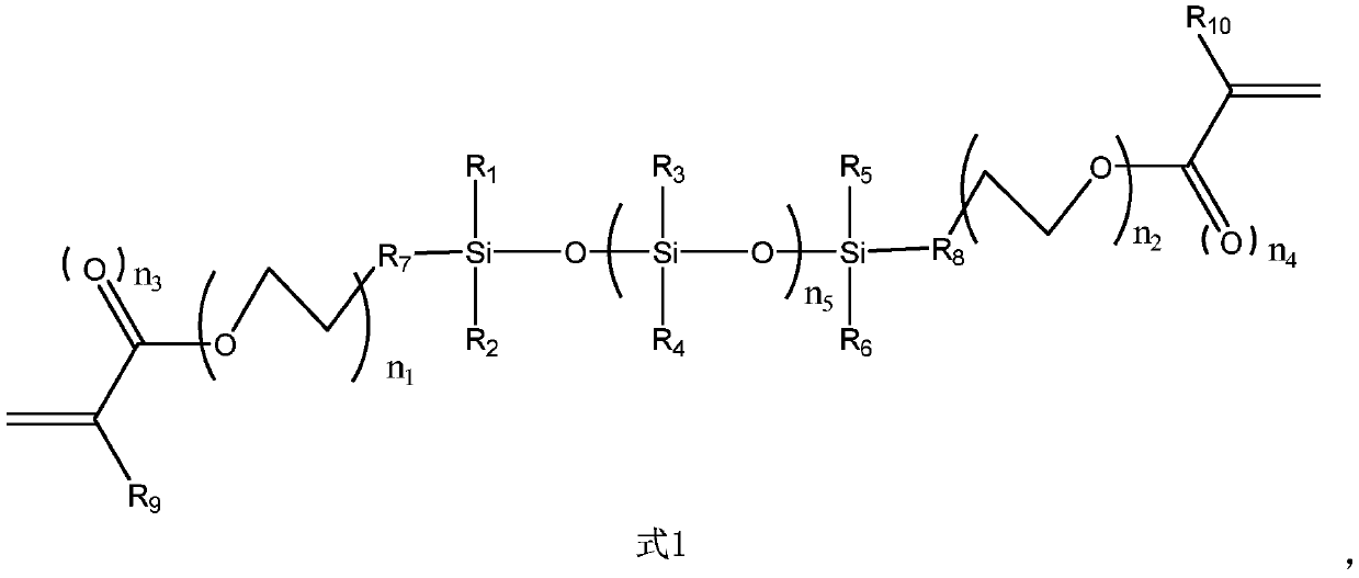
[0061] A compound L001, namely the compound numbered L001, the structure of the compound L001 is shown in formula 5:
[0062]
[0063] In this example, the steps of the preparation method of the compound L001 are as follows:
[0064] 1) Weigh 4g of diphenylsilanediol, 8g of (1,3-dimethyldisiloxane-1,1,3,3-tetrayl)tetrakis(propane-3,1-diyl)tetra( 2-methyl acrylate) and 0.6g of p-toluenesulfonic acid were added to a 50mL three-necked flask, stirred for 40 hours, then dissolved in 100mL of toluene, and washed 5 times with deionized water in a separatory funnel; then by rotary evaporation Toluene was removed to obtain the compound L001: (1,5-dimethyl-3,3-diphenyltrisiloxane-1,1,5,5-tetrayl)tetrakis(propane-3,1-di base) tetrakis (2-methyl acrylate) (58% yield).
Embodiment 2
[0066] Weigh 50g of the monomer of the compound L001 prepared by the preparation method in Example 1, mix it with an appropriate amount of component B and 20g of component C, stir at 50°C for 80h under vacuum, and then use a syringe filtering through a filter to obtain the composition for encapsulating photoelectric devices.
[0067] Among them, the component B includes 640g of 2-methyl-2-acrylic acid-1,12-dodecanediol ester and 290g of acrylic acid 2-([1,1′-biphenyl]-2-2-oxo base) ethyl acrylate, and the component C is a photoinitiator 2,4,6-trishydroxymethylbenzoyl diphenylphosphine oxide.
[0068] In this embodiment, the composition for encapsulating optoelectronic devices is coated with a spray agent, according to 100mW / cm 2 Under the conditions of about 10 seconds of irradiation, harden with ultraviolet light to form a coating with a coating thickness of 3 μm; the coating is used as an organic layer (i.e. an organic film), and silicon nitride is used as an inorganic laye...
Embodiment 3
[0070] Compared with Example 2, except that the mass of the monomer of the compound L001 is replaced by 100g, the mass of the 2-methyl-2-acrylic acid-1,12-dodecanediol ester is replaced by 615g, and the The mass of 2-([1,1′-biphenyl]-2-2-oxyl)ethyl acrylate was replaced with 265g, and the others were the same as in Example 2.
PUM
| Property | Measurement | Unit |
|---|---|---|
| thickness | aaaaa | aaaaa |
Abstract
Description
Claims
Application Information
 - R&D Engineer
- R&D Manager
- IP Professional
- Industry Leading Data Capabilities
- Powerful AI technology
- Patent DNA Extraction
Browse by: Latest US Patents, China's latest patents, Technical Efficacy Thesaurus, Application Domain, Technology Topic, Popular Technical Reports.
© 2024 PatSnap. All rights reserved.Legal|Privacy policy|Modern Slavery Act Transparency Statement|Sitemap|About US| Contact US: help@patsnap.com


