Normally-equipped integrated unit diode chip
An integrated unit and diode technology, applied in electrical components, electrical solid devices, circuits, etc., can solve the problems of LED light efficiency, heat dissipation and stability limitations, and achieve improved light extraction efficiency, large heat dissipation area, and high photoelectric conversion efficiency. Effect
- Summary
- Abstract
- Description
- Claims
- Application Information
AI Technical Summary
Problems solved by technology
Method used
Image

Examples
Embodiment 1
[0037] This embodiment provides a 6V high-voltage integrated unit light-emitting diode chip design, such as Figure 12-13 As shown, every two chip units are connected in series with each other to form a 6V high-voltage chip unit, and each 6V high-voltage chip unit is connected in parallel with each other. At this time, the ratio of series-parallel connection is 1:1. The units are connected in series with each other, and then connected in parallel with other N chip units. At this time, the ratio of series-parallel connection is 1:N. The circuit diagram is as follows Figure 12 shown.
[0038] Such as Figure 13As shown, the 6V high-voltage chip units are insulated from each other, and the n-type gallium nitride (n-GaN) platform 7 is exposed for each unit, and the left chip is connected in series through the bridge metal in the middle. The n-electrode and the p-electrode of the chip on the right. The 6V chip units are connected in parallel with each other, so even if a certai...
Embodiment 2
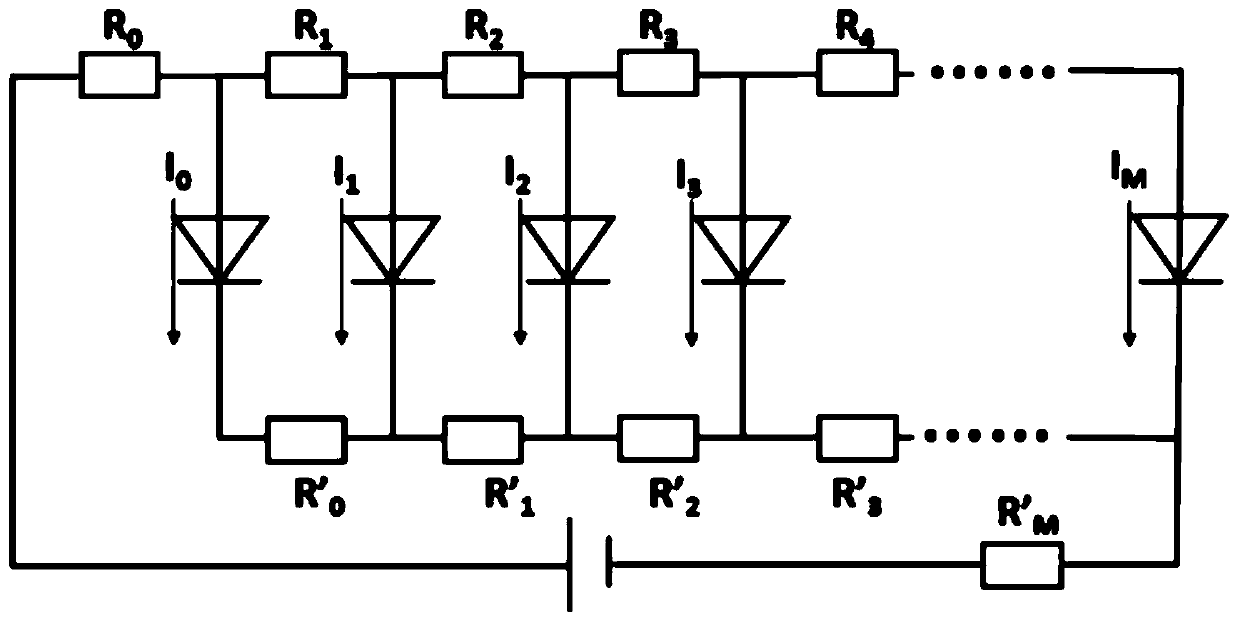
[0042] This embodiment provides a formal integration design method, image 3 It is a schematic circuit diagram of the unit diode chip series structure of the present invention.
[0043]
[0044] where R 0 , R 1 , R 2 , R 3 , R 4 ... is the resistance from the P-type electrode electrode line between a plurality of unit diode chips to the quantum well active region; R' 0 , R' 1 , R' 2 , R' 3 , R' 4 ...is the resistance from the N-type electrode electrode line between the multiple unit diode chips to the active region of the quantum well. Usually in the Nth unit diode chip, R N =R NM +R Nc +R Np-GaN , where R NM is the electrode wire resistance of the P-type electrode, R Nc is the contact resistance of a p-type ohmic contact, R Np-GaN is the resistance of p-GaN material; similarly, in the Nth unit diode chip, R′ N =R' NM +R' Nc +R' Nn-GaN , where R' NM is the electrode wire resistance of N-type electrode, R' Nc is the contact resistance of n-type ohmic co...
Embodiment 3
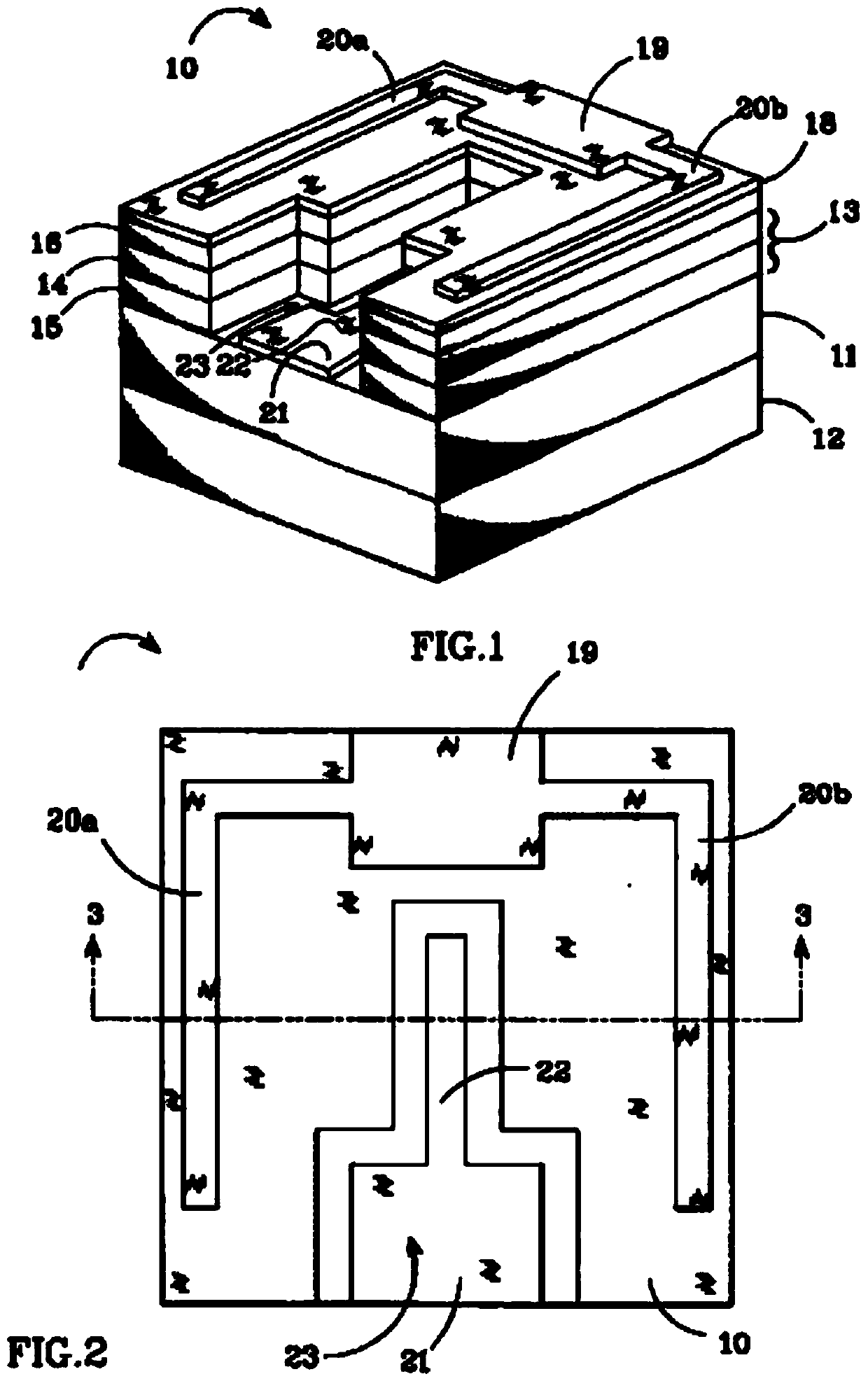
[0053] This embodiment provides a positively mounted integrated unit diode chip, the mesa structure area of which is determined according to the current, such as Figure 5 to Figure 7 As shown, it includes N-type electrode 1 , P-type electrode 2 , ITO 3 , hole 11 , N-type electrode line 12 , and P-type electrode line 13 .
[0054] In the unit diode chip, the length of the diode unit row is fixed as L, and the diode units from the P-type electrode to the right are defined in sequence, and their widths are defined as L 0 , L 1 , L 2 , L 3 ,... L N …L M ; where the width of the diode unit satisfies L 0 >L 1 >L 2 >L 3 >…>L N ...> L M , the optimal design approximation is:
[0055]
[0056] According to L N And the area calculation formula to calculate the area of the mesa structure.
[0057] In this embodiment, the front sectional view of the hole structure is added as Figure 5 As shown, the pore structure includes a plurality of pore units, the number of por...
PUM
| Property | Measurement | Unit |
|---|---|---|
| diameter | aaaaa | aaaaa |
| diameter | aaaaa | aaaaa |
Abstract
Description
Claims
Application Information
 - R&D
- Intellectual Property
- Life Sciences
- Materials
- Tech Scout
- Unparalleled Data Quality
- Higher Quality Content
- 60% Fewer Hallucinations
Browse by: Latest US Patents, China's latest patents, Technical Efficacy Thesaurus, Application Domain, Technology Topic, Popular Technical Reports.
© 2025 PatSnap. All rights reserved.Legal|Privacy policy|Modern Slavery Act Transparency Statement|Sitemap|About US| Contact US: help@patsnap.com