Optical frequency response electron tunneling structure as well as preparation method and application thereof
A technology of electron tunneling and optical frequency, applied in the field of optical frequency response, can solve the problem of low efficiency of optical frequency response
- Summary
- Abstract
- Description
- Claims
- Application Information
AI Technical Summary
Problems solved by technology
Method used
Image
Examples
Embodiment 1
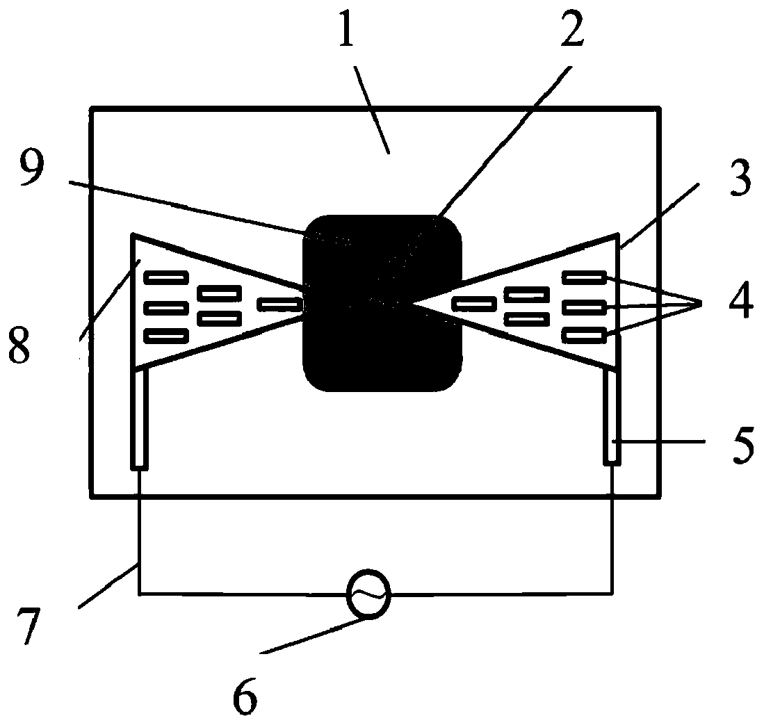
[0092] An optical frequency-responsive electron tunneling device using gold nanoribbons to enhance the electron tunneling process (for a schematic diagram of its structure, see figure 1 ):
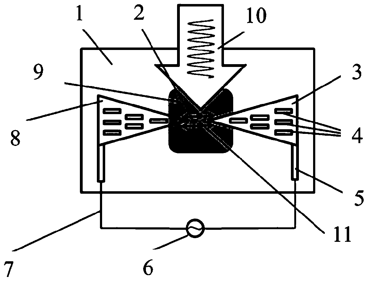
[0093] In the structure of the optical frequency response electron tunneling device in this embodiment: the substrate 1 is SiO 2 The substrate, the electron tunneling tip 2 is a carbon nanotube with a diameter of 5 nm, the first substrate in the upper electrode 3 is an Au electrode, the nano-enhanced structure 4 is an Au nano-strip, and the in-plane lead 5 is an Al in-plane electrode. The collector 6 is a Keithley Naan ammeter, the external lead 7 is a Cu wire, the second substrate in the lower electrode 8 is the lower Au electrode, and the nano-tunneling layer 9 is Al 2 o 3 Nano tunneling layer;
[0094] Among them, Al 2 o 3 The thickness of the tunneling layer is 1 nanometer, the bow-tie optical antenna, the side length of a single regular triangle is 300nm, the diameter of the elec...
Embodiment 2
[0104] An optical frequency-responsive electron tunneling device using carbon nanotips to enhance the electron tunneling process:
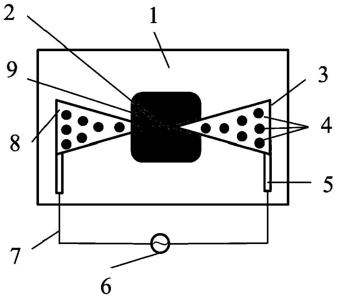
[0105] The structure of the optical frequency response electron tunneling device in this embodiment is as follows image 3 As shown in the figure: substrate 1 is Al 2 o 3 The substrate, the electron tunneling tip 2 is a carbon nano tip, the first substrate in the upper electrode 3 is an upper Ag electrode, the nano-enhanced structure 4 is an Al nanoparticle, the in-plane lead 5 is an Au in-plane electrode, and the current detection and collector 6 It is a Keithley Naan ammeter, the external lead 7 is a Cu wire, the second substrate in the lower electrode 8 is a lower Ag electrode, and the nano-tunneling layer 9 is Al 2 o 3 Nanotunneling layer.
[0106] Among them, Al 2 o 3 The thickness of the tunneling layer is 5 nanometers, the diameter and length of the carbon nanometer tip are 1nm and 5 μm respectively, the characteristic size of the upp...
PUM
| Property | Measurement | Unit |
|---|---|---|
| Thickness | aaaaa | aaaaa |
| Diameter | aaaaa | aaaaa |
| Thickness | aaaaa | aaaaa |
Abstract
Description
Claims
Application Information
 - R&D
- Intellectual Property
- Life Sciences
- Materials
- Tech Scout
- Unparalleled Data Quality
- Higher Quality Content
- 60% Fewer Hallucinations
Browse by: Latest US Patents, China's latest patents, Technical Efficacy Thesaurus, Application Domain, Technology Topic, Popular Technical Reports.
© 2025 PatSnap. All rights reserved.Legal|Privacy policy|Modern Slavery Act Transparency Statement|Sitemap|About US| Contact US: help@patsnap.com


