


Quick Research
Generate reliable direction feasibility study reports for your R&D in just a few steps.

Technical Q&A
Discover and master advanced knowledge NOW. Basics, ideas, possibilities, all at once.

Find Solutions
As an expert in R&D theories, this can generate solutions to your technical problems instantly.

Evaluate Feasibility
Analyze your overall solution with one click, know your potential R&D risks in advance.

Monitor Landscape
Get weekly tech updates, stay abreast of the latest tech innovations and key insights.
High-precision circuit board and manufacturing method thereof
A circuit board, high-precision technology, applied in the direction of printed circuit manufacturing, circuit substrate materials, printed circuits, etc., can solve the problems of high graphics accuracy, limited circuit density of printed circuit boards, and difficult to achieve
- Summary
- Abstract
- Description
- Claims
- Application Information
AI Technical Summary
Problems solved by technology
Method used
Image


Examples
Embodiment 1
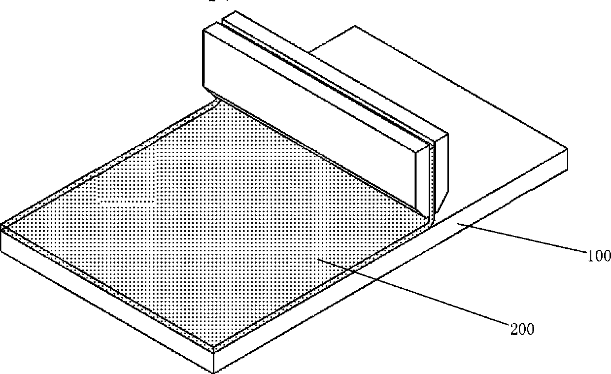
[0028] Such as figure 1 As shown, this high-precision circuit board includes a support base 1 and a conductive circuit 2 arranged on the support base 1. The support base 1 is a polyimide film 200 formed on a flat mother glass 100, and the conductive circuit 2 is The metal layer 300, the metal layer 300 has the corresponding pattern of the conductive circuit 2, the formation conditions of the metal layer 300 include that the support base 1 is on the flat mother glass 100, the metal layer 300 is deposited on the support base 1 by magnetron sputtering, the metal layer 300 forms the corresponding pattern of the conductive circuit 2 through a photolithography process.
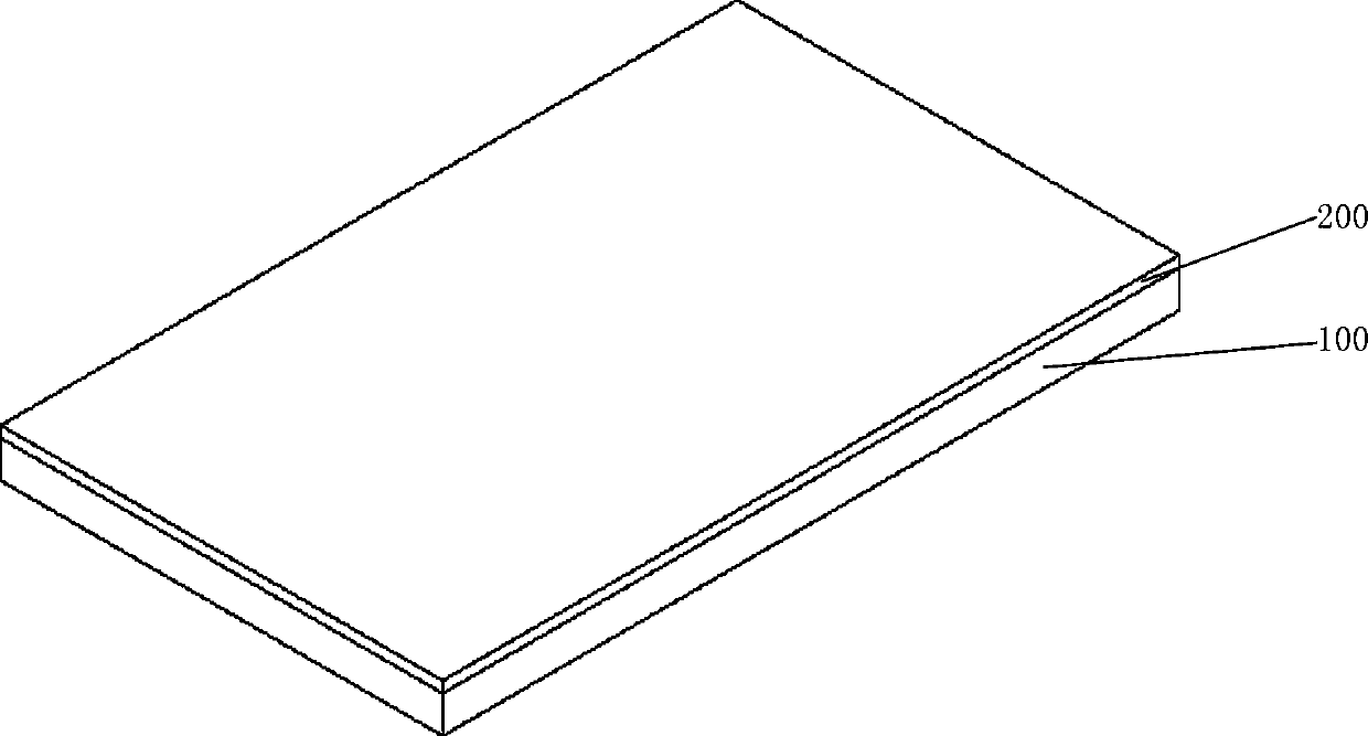
[0029] The thickness of the above-mentioned polyimide film 200 may be 10 μm˜100 μm. The above-mentioned flat mother glass 100 is preferably float glass with very high flatness, which can ensure that the formed polyimide film 200 has high flatness (thickness uniformity) and high smoothness.
[0030] In this embodim...
Embodiment 2
[0048] Such as Figure 8 As shown, in the case that other parts are the same as the first embodiment, the difference is that the conductive circuit 2 includes a first wire layer 201 and a second wire layer 202, and a There is an insulating isolation layer 5, and the isolation layer 5 is a patterned photosensitive resin coating; the isolation layer 5 is provided with a through hole 6, and the first wire layer 201 and the second wire layer 202 are connected to each other through the through hole 6. .
[0049] Specifically, it is preferred that the isolation layer 5 is a photosensitive resin layer coated by spin coating, flat coating (or extrusion coating, slit coating), which has good thickness uniformity and smoothness, and its thickness can be 0.5 μm ~5μm. The isolation layer 5 is preferably patterned using a yellow light process (i.e., exposure and development), and its pattern accuracy can also reach a level above 10 μm, so it can be matched with high-precision lines and r...
PUM
| Property | Measurement | Unit |
|---|---|---|
| thickness | aaaaa | aaaaa |
| thickness | aaaaa | aaaaa |
Abstract
Description
Claims
Application Information
 - R&D Engineer
- R&D Manager
- IP Professional
- Industry Leading Data Capabilities
- Powerful AI technology
- Patent DNA Extraction
Browse by: Latest US Patents, China's latest patents, Technical Efficacy Thesaurus, Application Domain, Technology Topic, Popular Technical Reports.
© 2024 PatSnap. All rights reserved.Legal|Privacy policy|Modern Slavery Act Transparency Statement|Sitemap|About US| Contact US: help@patsnap.com