
PCB double-sided board grinding device for electronic product and working method thereof

A technology for electronic products and PCB boards, which is applied in the field of PCB double-sided grinding board devices for electronic products, can solve the problems of difficult removal of resin chips, low grinding efficiency, and PCB board fixation, so as to reduce the contact area and the clamping effect. Good, simple structure

Active Publication Date: 2020-03-24
江苏百维能源科技有限公司
View PDF17 Cites 6 Cited by
  • Summary
  • Abstract
  • Description
  • Claims
  • Application Information

AI Technical Summary

Problems solved by technology

[0003] The patent document (201410036892.0) discloses a PCB board grinding machine, which has a simple structure and is easy to operate. By adjusting the distance between the grinding board assembly and the PCB board, the adjustment of the grinding amount can be realized, so that the different heights of the PCB board can be obtained. Proper grinding, so as to avoid excessive grinding of the higher part of the PCB board and expose the base material or the lower part of the PCB board is not polished and the resin is not completely worn off, but the grinding machine is facing the double-layer PCB When grinding the board, it needs to be polished twice before and after, and the grinding efficiency is not high. At the same time, the board grinding machine cannot fix PCB boards of different sizes and thicknesses, and the resin chips generated during the grinding process are also difficult to remove.

Method used


Image

  • PCB double-sided board grinding device for electronic product and working method thereof
  • PCB double-sided board grinding device for electronic product and working method thereof
  • PCB double-sided board grinding device for electronic product and working method thereof

Examples


Embodiment Construction

[0034] The following will clearly and completely describe the technical solutions in the embodiments of the present invention with reference to the accompanying drawings in the embodiments of the present invention. Obviously, the described embodiments are only some, not all, embodiments of the present invention. Based on the embodiments of the present invention, all other embodiments obtained by persons of ordinary skill in the art without creative efforts fall within the protection scope of the present invention.

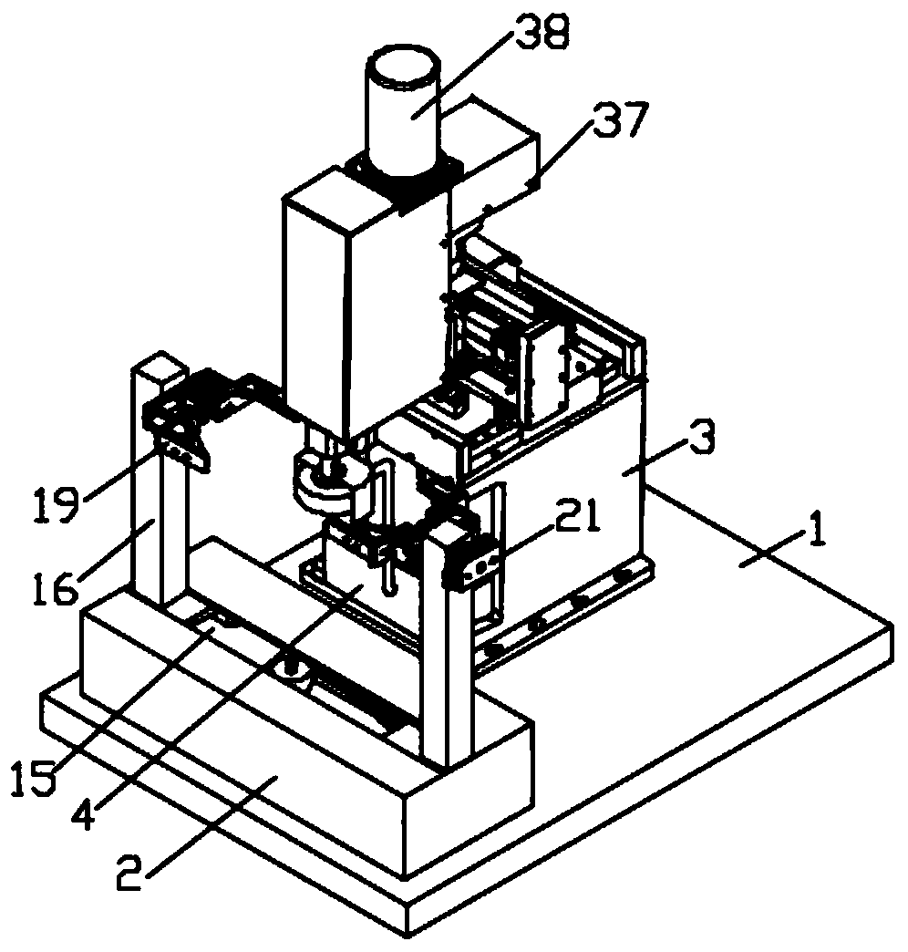
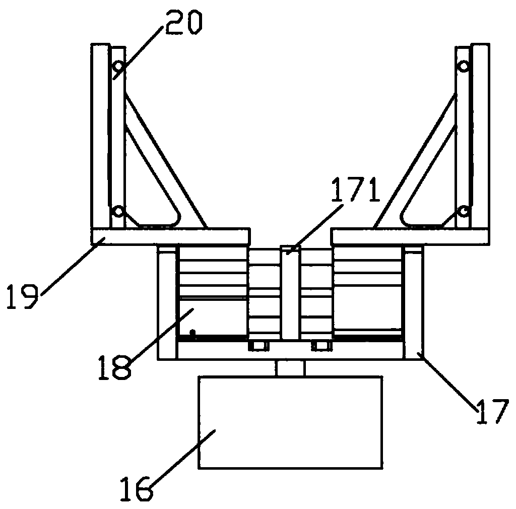
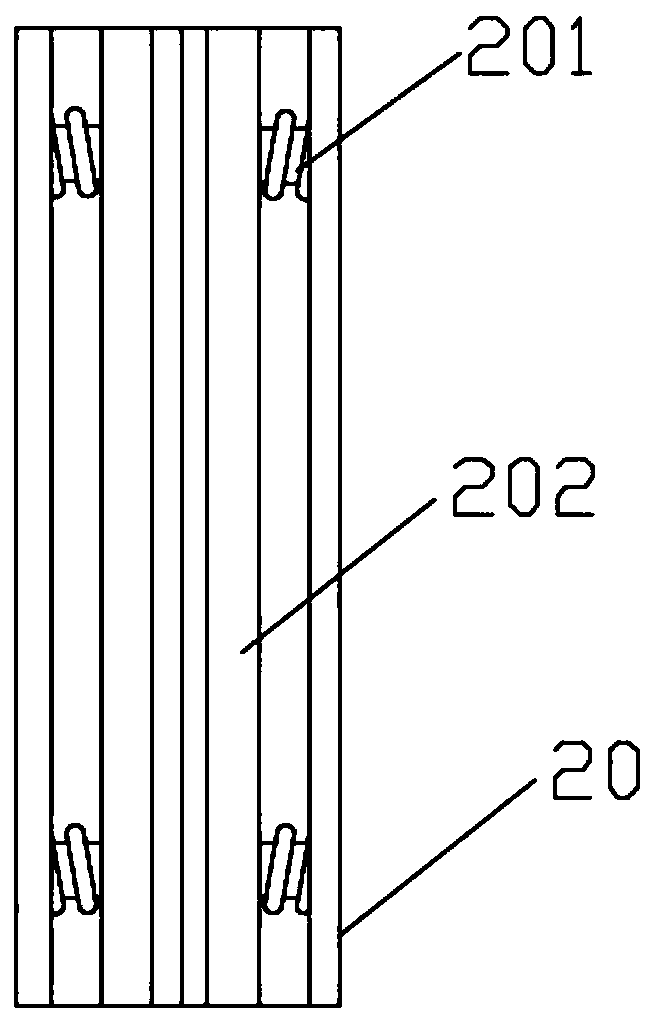
[0035] see Figure 1-7 As shown, the present invention is a PCB double-sided board grinding device for electronic products, including a machine platform 1, a clamping seat 2, a grinding platform 3 are arranged on the machine platform 1, a chip collection box 4 is installed on the grinding platform 3, and a clip The holding seat 2 is a rectangular box structure, and a fixing plate 14 is installed in the holding seat 2, and a first cylinder 5 is also arranged in the ...


PUM


Abstract

The invention discloses a PCB double-sided board grinding device for an electronic product and a working method thereof. The device comprises a machine table, wherein a clamping seat and a grinding table are arranged on the machine table, a chip collecting box is mounted on the grinding table, the clamping seat is of a rectangular box body structure, a fixing plate is mounted in the clamping seat,a first air cylinder is further arranged in the clamping seat, and a piston rod of the first air cylinder is connected with a connecting strip. According to the device, the first cylinder piston rodis contracted, so that one mounting plate is driven to move through the connecting strip, the mounting plate drives a rod sleeve to slide on a fixing rod, then a clamping strip drives a rotating wheeland a limiting rolling wheel to rotated, the rotating wheel drives the other clamping strip to move, the two clamping strips are driven to move towards each other, and then two moving side columns are driven to move towards each other through the two mounting plates, so that the technical problem that the PCB board grinding device is prone to be stuck due to the conventional screw rod adjusting clamping in the prior art is solved.

Description

technical field [0001] The invention relates to the technical field of PCB board production, in particular to a PCB double-sided board grinding device for electronic products and a working method thereof. Background technique [0002] PCB board, also known as printed circuit board, is the provider of electrical connection for electronic components. According to the number of layers of circuit boards, PCB boards can be divided into single-sided boards, double-sided boards, four-layer boards, six-layer boards and other multi-layer circuit boards. With the progress of vlsi, miniaturization and high integration of electronic components, multi-layer boards are mostly moving towards the direction of matching high-function circuits. Therefore, the demand for high-density circuits and high wiring capacity is increasing. PCB double-sided panels are used in There are more and more electronic products, because there are traces on both sides of the PCB board, and both sides need to be ...

Claims


Application Information

Patent Timeline
Patent Type & Authority Applications(China)
IPC IPC(8): B24B7/10B24B55/06B24B41/06B24B47/06B24B47/12B24B41/02B24B27/00H05K3/00
CPCB24B7/10B24B27/0046B24B41/02B24B41/068B24B47/06B24B47/12B24B55/06H05K3/00
Inventor 王大榕汪建军辛园庆王星王婷
Owner 江苏百维能源科技有限公司
Learn More