
Radiation-proof reinforced circuit for a CMOS standard unit

An anti-radiation hardening, standard cell technology, applied in logic circuits, electrical components, reliability improvement and modification, etc., can solve problems such as permanent device damage, semiconductor device flipping, device gate oxide breakdown, etc., and achieve a small area overhead , the effect of improving the ability to resist single-event flipping

Pending Publication Date: 2020-03-13
UNIV OF ELECTRONIC SCI & TECH OF CHINA
View PDF6 Cites 1 Cited by
  • Summary
  • Abstract
  • Description
  • Claims
  • Application Information

AI Technical Summary

Problems solved by technology

When the sensitive area of ​​a semiconductor device is bombarded by a single high-energy particle from the outside, it will ionize on its trajectory to generate electron-hole pairs. Once these ionized charges are collected by the electrodes of the semiconductor device, it will cause the original logic level of the semiconductor device to change. flipping or permanent damage to the device
In other words, if a single event effect occurs, it will definitely cause a transient disturbance, which may cause the flipping of the memory cell, the latch-up of the device, and even the breakdown of the gate oxide of the device, the burning of the circuit, etc.

Method used


Image

  • Radiation-proof reinforced circuit for a CMOS standard unit
  • Radiation-proof reinforced circuit for a CMOS standard unit
  • Radiation-proof reinforced circuit for a CMOS standard unit

Examples


Embodiment Construction

[0019] In order to make the technical solutions and advantages of the present invention clearer, the present invention will be further described in detail below in conjunction with specific embodiments and with reference to the accompanying drawings.

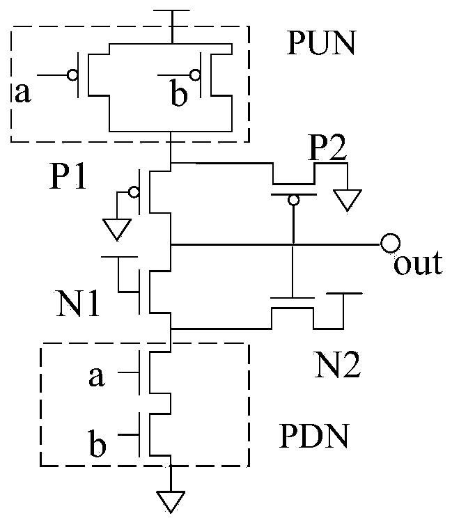
[0020] figure 1 It is a schematic diagram for explaining the CMOS standard cell reinforcement circuit of the present invention, including PUN network, PDN network, p-type channel field effect transistor P1, p-type channel field effect transistor P2, n-type channel field effect transistor N1, n-type channel field effect transistor Transistor N2.

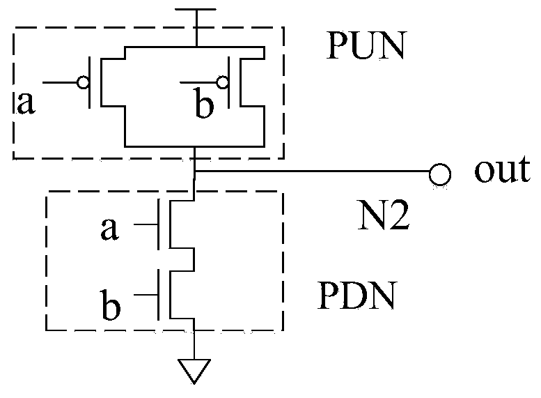
[0021] figure 2 It is a reinforced two-input NAND gate, the gate of P1 tube is connected to low level, the source of P1 is connected to PUN network, the drain of P1 tube is connected to the output port; the gate of N1 tube is connected to high level, and the drain of N1 tube is connected to the output port. The port is connected, and the source of the N1 tube is connected to the PDN ...


PUM


Abstract

The invention discloses a radiation-proof reinforced circuit for a CMOS standard unit. The radiation-proof reinforced circuit comprises a pull-up network (PUN) and a pull-down network (PDN) for realizing a logic function, two p-type channel field effect transistors P1 and P2, and two n-type channel field effect transistors N1 and N2. Figure 1 shows a universal logic gate unit with N inputs, and all inputs of the logic gate unit are simultaneously distributed to pull-up and pull-down networks. The grid electrode of a P1 is connected with a low level, and the grid electrode of an N1 is connectedwith a high level. The grid electrode of a P2 is connected with the output port, the source electrode is connected with the source electrode of P1, the drain electrode is connected with low level, the grid electrode of N2 is connected with the output port, the drain electrode is connected with high level, and the source electrode is connected with the drain electrode of N1. The sensitive nodes ofthe standard unit are subjected to radiation-proof reinforcement, so that the single event upset resisting effect of the standard unit is obviously improved on the premise that the area overhead is not large.

Description

technical field [0001] The invention relates to the technical field of anti-single-event reversal reinforcement of a CMOS standard cell library. Background technique [0002] The space radiation environment refers to the complex radiation environment caused by various cosmic rays and solar activities existing in the atmosphere and space, mainly including Van Allen radiation belts, cosmic rays and solar radiation. [0003] When a semiconductor device is bombarded by high-energy particles from the space environment, the high-energy particles will interact with the semiconductor material and ionize to generate electron-hole pairs, so that the device or circuit will respond differently, resulting in failure or failure. [0004] The single event effect, in simple terms, is the immediate effect produced after a single particle of a certain energy is injected into a semiconductor device. When the sensitive area of ​​a semiconductor device is bombarded by a single high-energy parti...

Claims


Application Information

Patent Timeline
IPC IPC(8): H03K19/003
CPCH03K19/00338
Inventor 张黛梦谢小东陈飞翔
Owner UNIV OF ELECTRONIC SCI & TECH OF CHINA
Learn More