Latch preventing dual-node-flipping
A dual-node inversion and latch technology is applied in fields such as reliability improvement of field effect transistors, logic circuit coupling/interface using field effect transistors, and reliability improvement modification. Problems such as double-node flipping achieve low area overhead, improved ability to resist single event flipping, and high reliability
- Summary
- Abstract
- Description
- Claims
- Application Information
AI Technical Summary
Problems solved by technology
Method used
Image
Examples
Embodiment 1
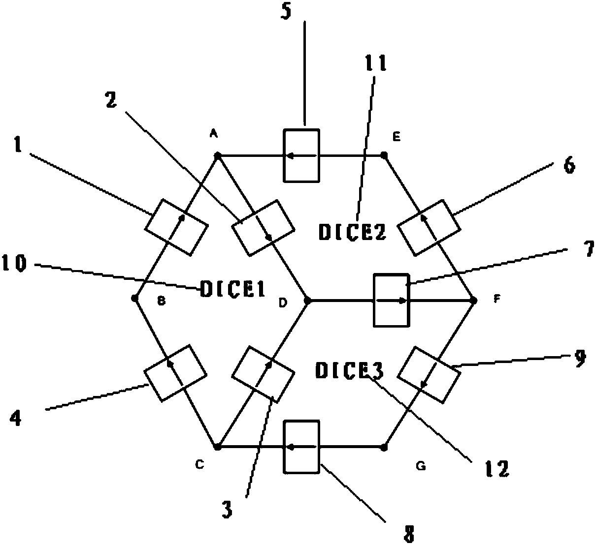
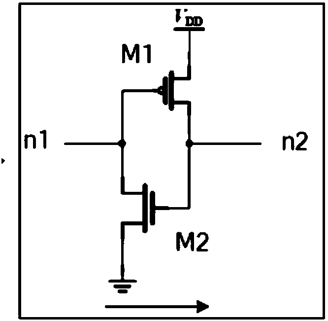
[0027] figure 1 It is a schematic structural diagram of a latch resistant to double-node flipping provided by an embodiment of the present application. Such as figure 1 shown, the latch consists of:
[0028] The latch has a storage node A, a storage node B, a storage node C, a storage node D, a storage node E, a storage node F, and a storage node G;
[0029] Specifically, a latch (Latch) is a memory unit circuit sensitive to a pulse level, and they can change states under the action of a specific input pulse level. Latch is to temporarily store the signal to maintain a certain level state. The main function of the latch is to cache, secondly to complete the asynchronous problem between the high-speed controller and the slow peripheral, then to solve the problem of the driver, and finally to solve the problem that an I / O port can output and input question. A latch is an input that uses level control data, and it includes a latch without enable control and a latch with enab...
Embodiment 2
[0038] In order to further explain the anti-double-node flipping latch provided in the present application, the embodiment of the present application describes the working principle of the anti-double-node flipping latch.
[0039] When the latch is in conduction mode, as Figure 4 As shown, the input data In are transmitted to storage node A, storage node C and storage node F through CMOS transmission gates TG1, TG2 and TG3 respectively, while storage node B, storage node D, storage node E and storage node G are connected with the input data In is logically the opposite. D is output to the output node Q through a clocked inverter, so the input In is logically the same as the output Q. In holdover mode, these redundant nodes have the ability to restore the correct logic. As a result, when the dual-node flip occurs, it can be restored to the normal logic level by the remaining storage nodes, which improves the ability of digital integrated circuits to resist single-event flipp...
PUM
 Abstract
Description
Claims
Application Information
 - Generate Ideas
- Intellectual Property
- Life Sciences
- Materials
- Tech Scout
- Unparalleled Data Quality
- Higher Quality Content
- 60% Fewer Hallucinations
Browse by: Latest US Patents, China's latest patents, Technical Efficacy Thesaurus, Application Domain, Technology Topic, Popular Technical Reports.
© 2025 PatSnap. All rights reserved.Legal|Privacy policy|Modern Slavery Act Transparency Statement|Sitemap|About US| Contact US: help@patsnap.com


