Light-emitting sign with metal surface effect and preparation method thereof
A technology of metal surface and production method, which is applied in the direction of illuminated signs, instruments, display devices, etc., can solve the problems of non-compliance with environmental protection requirements, health threats of production personnel, etc., and achieve excellent weather aging resistance, consistency, and resources. saving effect
- Summary
- Abstract
- Description
- Claims
- Application Information
AI Technical Summary
Problems solved by technology
Method used
Image
Examples
Embodiment 1
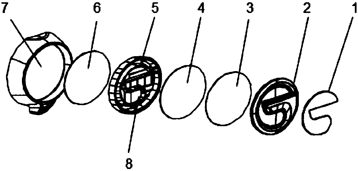
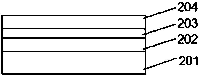
[0031] Such as figure 1 and figure 2 As shown, a luminous sign with a metal surface effect includes a shading plate 1, an ePVD metal sign 2, a diffuser plate 3, a light guide plate 4, a reflective frame 5, a PCBA light plate 6, and a base 7 arranged in sequence from top to bottom. The reflective frame 5 is provided with a reflective cavity 8, and the PCBA lamp board 6 is provided with an LED lamp and an LED lamp drive circuit, and the LED lamp drive circuit is connected to the LED lamp 9 through wires; among them, 60 LED lamps are uniformly arranged on the PCBA board 9. The back of the shading plate 1 is ultrasonically welded to the front of the ePVD metal sign 2, the back of the ePVD metal sign 2 is ultrasonically welded to the front of the diffuser plate 3, the back of the diffuser 3 is connected to the front of the light guide plate 4 by buckles, and the back of the light guide plate 4 is connected to the reflector The front of the frame 5 is connected by a buckle, the ba...
Embodiment 2
[0035] A method of making a luminous sign with a metal surface effect in Example 1 is as follows:
[0036] S1. Injection molding of signboard base material: the ABS material is made into the signboard body by injection molding;
[0037] S2. Pretreatment of signboard base material: performing dust removal and static electricity removal on the signboard body obtained in step S1;
[0038] S3, UV primer layer spraying: spraying a UV primer layer on the surface of the sign body treated in step S2, wherein the thickness of the UV primer layer is 10-15 μm;
[0039] S4. PVD coating: forming a chromium coating on the surface formed in step S3 by magnetron sputtering or vacuum evaporation, wherein the thickness of the chromium coating 203 is 0.1-0.2 μm.
[0040] S5. UV high-hardness coating: spray a UV high-hardness coating on the surface formed in step S4, wherein the thickness of the UV high-hardness topcoat layer 204 is 10-15 μm.
[0041] S6. Static removal: carry out static remova...
PUM
| Property | Measurement | Unit |
|---|---|---|
| thickness | aaaaa | aaaaa |
| thickness | aaaaa | aaaaa |
| thickness | aaaaa | aaaaa |
Abstract
Description
Claims
Application Information
 - R&D
- Intellectual Property
- Life Sciences
- Materials
- Tech Scout
- Unparalleled Data Quality
- Higher Quality Content
- 60% Fewer Hallucinations
Browse by: Latest US Patents, China's latest patents, Technical Efficacy Thesaurus, Application Domain, Technology Topic, Popular Technical Reports.
© 2025 PatSnap. All rights reserved.Legal|Privacy policy|Modern Slavery Act Transparency Statement|Sitemap|About US| Contact US: help@patsnap.com


