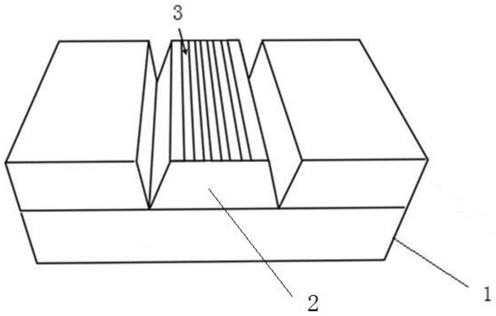
A waveguide grating coupler based on photothermosensitive refractive glass and its preparation method
A waveguide grating and photothermographic technology, applied in the field of integrated optics, can solve the problems of unseen waveguide grating coupler, difficult control of beam interference, etc., and achieve the effect of light weight, excellent optical characteristics, and high integration
- Summary
- Abstract
- Description
- Claims
- Application Information
AI Technical Summary
Problems solved by technology
Method used
Image
Examples
preparation example Construction
[0037] The present invention also discloses a method for preparing a waveguide grating coupler based on photothermosensitive refractive glass. The method includes the following steps:
[0038] S1: Sample pretreatment
[0039] Cut the photothermographic glass to a suitable size, perform optical polishing and cleaning on the surface;
[0040] Specifically, the PTR glass sample is cut to obtain a suitable size, and the surface to be processed is optically polished, and the polished sample needs to be cleaned before the ion implantation operation.
[0041] S2: Preparation of planar waveguide structure
[0042] Put the photothermographic glass sample cut in step S1 into the ion accelerator, select appropriate implantation conditions for ion implantation, and finally form a planar waveguide layer by ion bombardment on the surface of the sample.
[0043] The pretreated sample is ion-implanted to obtain a planar waveguide structure. In step S2, ion implantation includes light ion i...
Embodiment 1
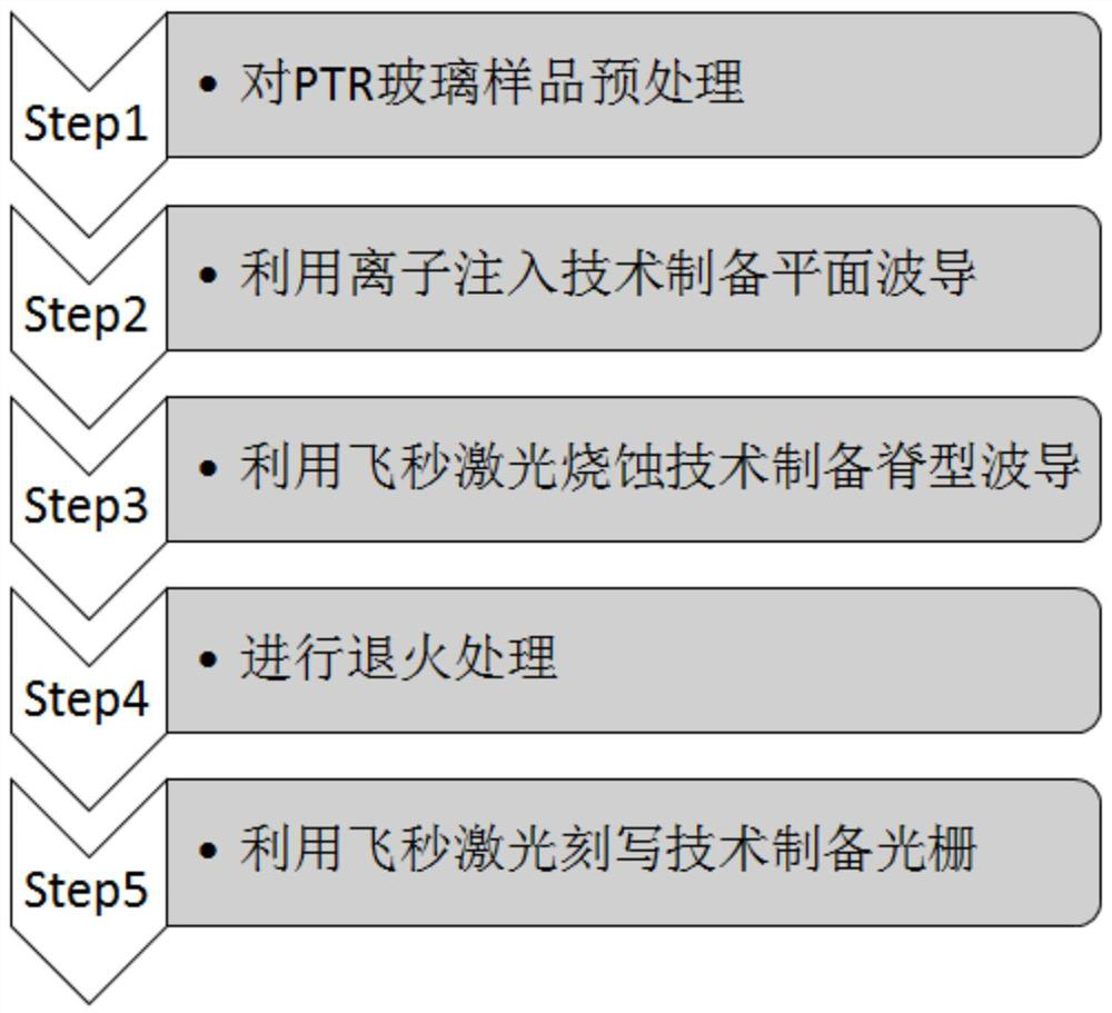
[0057] according to figure 2 The preparation process schematic diagram carries out the following steps successively:
[0058] (1) First cut the sample PTR glass into a size of 10.0×5.0×1.0mm 3 , and to 10.0 x 5.0mm 2 The surface of the sample is optically polished, and then the polished sample is cleaned with acetone, ethanol and deionized water to remove surface impurities to meet the requirements of subsequent ion implantation to form an optical waveguide.
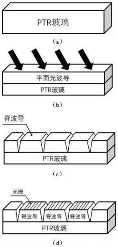
[0059] (2) Use an ion beam accelerator with an energy of 400keV and a dose of 4.0×10 16 ions / cm 2 hydrogen ions, so that the hydrogen ions are implanted into the PTR glass to form a planar waveguide, such as image 3 (b) shown.
[0060] (3) Femtosecond laser pulse longitudinal ablation is used on the planar optical waveguide prepared by ion implantation, such as Figure 4 shown. A femtosecond laser with a center wavelength of 800 nm, a pulse width of 220 fs, and a pulse repetition frequency of 1 kHz is focused on...
Embodiment 2
[0064] according to figure 2 The preparation process schematic diagram carries out the following steps successively:
[0065] (1) The size of the sample PTR glass after cutting is 10.0×5.0×1.0mm 3 , and optically polish the upper surface of the cut sample PTR glass; the polished sample needs to be cleaned to remove surface impurities.
[0066] (2) Passing energy is 6MeV, dose is 5.0×10 14 ions / cm 2 Carbon ions are implanted into the cleaned PTR sample to form a planar waveguide, the structure is as follows image 3 (b) shown.
[0067] (3) A ridge-shaped waveguide structure is prepared on the planar optical waveguide by femtosecond laser ablation technology, so that it limits the propagation of light in two dimensions. Place the sample on a three-dimensional mobile platform controlled by a computer, use the Ti:Sapphire laser system to output femtosecond laser pulses with a central wavelength of light source of 800nm, a repetition rate of 1kHz, and a pulse width of 220fs, ...
PUM
 Abstract
Description
Claims
Application Information
 - R&D
- Intellectual Property
- Life Sciences
- Materials
- Tech Scout
- Unparalleled Data Quality
- Higher Quality Content
- 60% Fewer Hallucinations
Browse by: Latest US Patents, China's latest patents, Technical Efficacy Thesaurus, Application Domain, Technology Topic, Popular Technical Reports.
© 2025 PatSnap. All rights reserved.Legal|Privacy policy|Modern Slavery Act Transparency Statement|Sitemap|About US| Contact US: help@patsnap.com


