Electrolytic etching and electroplating synchronous manufacturing method for fine circuit of printed circuit board
A printed circuit board, fine circuit technology, applied in the direction of printed circuit manufacturing, printed circuits, electrical components, etc., can solve the problems of high resource consumption, inconsistent with the production concept, high production cost, and achieve good circuit quality and high regularity. , the effect of improving production efficiency
- Summary
- Abstract
- Description
- Claims
- Application Information
AI Technical Summary
Problems solved by technology
Method used
Image
Examples
Embodiment 1
[0049] In this example, the electrolyte composition of anode chamber 1 is copper chloride dihydrate: 30g / L, hydrochloric acid: 0.48mol / L, 2,4,6-triaminopyrimidine: 90mg / L, and the electrolyte of cathode chamber 2 is Jiangsu Bomin Electronics Co., Ltd. Ltd. Tudian Potion.
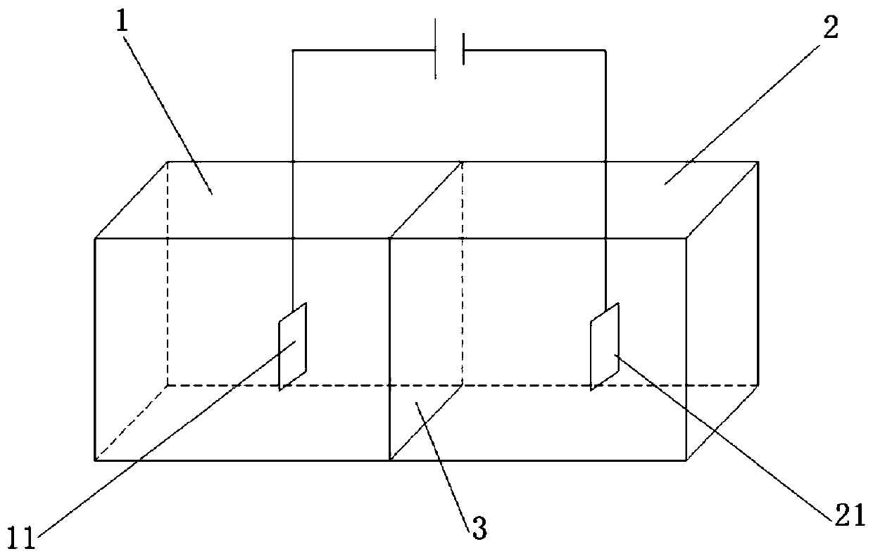
[0050] Using the above electrolytic solution to carry out electrolytic etching and electroplating thickening simultaneously, such as figure 1 As shown, the electrolytic cell is divided into an anode chamber 1 and a cathode chamber 2 by a cation exchange membrane 3, the electrolyte in the anode chamber 1 is the above-mentioned electrolytic etching solution, and the electrolyte in the cathode chamber 2 is CuSO 4 ﹒ 5H 2 O, H 2 SO 4 , Cl - , inhibitor, accelerator, with the circuit board to be electrolytically etched as the anode plate 11, and the circuit board to be thickened with equal area as the cathode plate 21, at a temperature of 30°C, the current density is 3.04A / dm 2 Under certain conditions, the ...
Embodiment 2
[0053] In this example, the electrolyte composition of anode chamber 1 is copper chloride dihydrate: 30g / L, hydrochloric acid: 0.48mol / L, 2,4,6-triaminopyrimidine: 90mg / L, and the electrolyte of cathode chamber 2 is Jiangsu Bomin Electronics Co., Ltd. Ltd. Tudian Potion.
[0054] Using the above electrolytic solution to carry out electrolytic etching and electroplating thickening simultaneously, such as figure 1 As shown, the electrolytic cell is divided into an anode chamber 1 and a cathode chamber 2 by a cation exchange membrane 3, the electrolyte in the anode chamber 1 is the above-mentioned electrolytic etching solution, and the electrolyte in the cathode chamber 2 is CuSO 4 ﹒ 5H 2 O, H 2 SO 4 , Cl - , inhibitor, accelerator, with the circuit board to be electrolytically etched as the anode plate 11, and the circuit board to be thickened with the same area as the cathode plate 21, at a temperature of 23°C, the current density is 3.04A / dm 2 Under certain conditions, t...
Embodiment 3
[0057] In this example, the electrolyte composition of anode chamber 1 is copper chloride dihydrate: 20g / L, hydrochloric acid: 0.36mol / L, 2,4,6-triaminopyrimidine: 90mg / L, and the electrolyte of cathode chamber 2 is Jiangsu Bomin Electronics Co., Ltd. Ltd. Tudian Potion.
[0058] Electrolytic etching and electroplating thickening are carried out simultaneously by using the above electrolyte, combined with the device figure 1 , the electrolytic cell is divided into an anode chamber 1 and a cathode chamber 2 with a cation exchange membrane 3, the electrolyte in the anode chamber 1 is the above-mentioned electrolytic etching solution, and the electrolyte in the cathode chamber 2 is CuSO 4 ﹒ 5H 2 O, H 2 SO 4 , Cl - , inhibitor, accelerator, with the circuit board to be electrolytically etched as the anode plate 11, and the circuit board to be thickened with the same area as the cathode plate 21, at a temperature of 23°C, the current density is 3.04A / dm 2 Under certain condit...
PUM
| Property | Measurement | Unit |
|---|---|---|
| thickness | aaaaa | aaaaa |
| thickness | aaaaa | aaaaa |
| thickness | aaaaa | aaaaa |
Abstract
Description
Claims
Application Information
 - R&D
- Intellectual Property
- Life Sciences
- Materials
- Tech Scout
- Unparalleled Data Quality
- Higher Quality Content
- 60% Fewer Hallucinations
Browse by: Latest US Patents, China's latest patents, Technical Efficacy Thesaurus, Application Domain, Technology Topic, Popular Technical Reports.
© 2025 PatSnap. All rights reserved.Legal|Privacy policy|Modern Slavery Act Transparency Statement|Sitemap|About US| Contact US: help@patsnap.com


