A method for growing large-scale zero-dimensional perovskite light-emitting single crystals
A large-size, perovskite technology, applied in the direction of single crystal growth, single crystal growth, crystal growth, etc., can solve the problems of cumbersome operation, serious pollution, and long time consumption, and achieve a wide luminous color gamut, low defect state density, Effect of High Carrier Mobility
- Summary
- Abstract
- Description
- Claims
- Application Information
AI Technical Summary
Problems solved by technology
Method used
Image
Examples
Embodiment 1
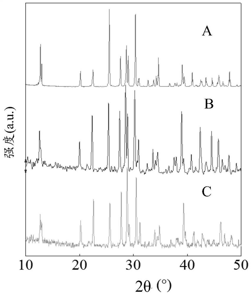
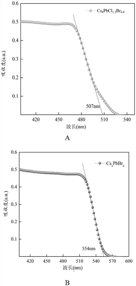
[0045] Lead cesium bromide and cesium chloride with a molar ratio of 1:1 were mixed and dissolved in DMSO respectively to obtain a mixed solution with a concentration of 0.1 mol / L. After the solution was fully stirred and uniform, the pure solution was sealed and transferred to a crystal growth tank to start growing crystals at 60°C. After spontaneous crystallization, the temperature was raised to 80°C at a rate of 1°C / min, and the crystal growth rate was controlled to about 1mm / day. Finally, a large-size zero-dimensional perovskite light-emitting single crystal with tunable band gap was obtained. for Cs 4 PbCl 1.2 Br 4.8 Single crystal, the size of the single crystal is about 4mm, the width at half maximum is 18nm, and the luminescence peak is 481nm. The physical photo of the single crystal is as follows figure 1 As shown in A. The crystal structure, absorption spectrum, luminescence spectrum and elemental analysis test results of the single crystal are as follows figur...
Embodiment 2
[0047] Lead cesium bromide and cesium bromide with a molar ratio of 1:1 were mixed and dissolved in DMSO respectively, so that the concentration of the mixed solution was 0.1 mol / L. After the solution was fully stirred and uniform, the pure solution was sealed and transferred to a crystal growth tank to start growing crystals at 60°C. After spontaneous crystallization, the temperature was raised to 80°C at 1°C / min, and the crystal growth rate was controlled to 1.5mm / day. Finally, a large-size zero-dimensional perovskite light-emitting single crystal with tunable band gap was obtained. for Cs 4 PbBr 6 Single crystal, the single crystal size is about 4mm, the full width at half maximum is 20nm, and the luminescence peak is 525nm. The real photo of the single crystal is shown in figure 1 Shown in B. The crystal structure, absorption spectrum, luminescence spectrum and elemental analysis test results of the single crystal are as follows figure 2 (Curve B), image 3 B. Fig...
Embodiment 3
[0049] Lead cesium bromide and cesium iodide with a molar ratio of 1:1 were mixed and dissolved in DMSO respectively, so that the concentration of the mixed solution was 0.1 mol / L. After the solution was fully stirred and uniform, the pure solution was sealed and transferred to a crystal growth tank to start growing crystals at 60°C. After spontaneous crystallization, the temperature was raised to 80°C at a rate of 1°C / min, and the crystal growth rate was controlled to about 1mm / day. Finally, a large-size zero-dimensional perovskite light-emitting single crystal with tunable band gap was obtained. for Cs 4 PB 0.3 Br 5.7 Single crystal, the single crystal size is about 4mm, the full width at half maximum is 18nm, and the luminescence peak is 536nm. The real photo of the single crystal is shown in figure 1 C shown. The crystal structure, absorption spectrum, luminescence spectrum and elemental analysis test results of the single crystal are as follows figure 2 (C curve), ...
PUM
| Property | Measurement | Unit |
|---|---|---|
| width | aaaaa | aaaaa |
| size | aaaaa | aaaaa |
| size | aaaaa | aaaaa |
Abstract
Description
Claims
Application Information
 - R&D
- Intellectual Property
- Life Sciences
- Materials
- Tech Scout
- Unparalleled Data Quality
- Higher Quality Content
- 60% Fewer Hallucinations
Browse by: Latest US Patents, China's latest patents, Technical Efficacy Thesaurus, Application Domain, Technology Topic, Popular Technical Reports.
© 2025 PatSnap. All rights reserved.Legal|Privacy policy|Modern Slavery Act Transparency Statement|Sitemap|About US| Contact US: help@patsnap.com


