
Silicon-based multimode helical waveguide delay line supporting low-loss fundamental mode transmission

A helical wave and delay line technology, applied in the field of silicon-based multi-mode helical waveguide delay lines, can solve the problems of long propagation distance, compact structure, mismatch loss between modes, etc., achieve compact structure, reduce electric field strength, and fundamental mode transmission. Low loss effect

Active Publication Date: 2019-12-20
ZHEJIANG UNIV
View PDF6 Cites 12 Cited by
  • Summary
  • Abstract
  • Description
  • Claims
  • Application Information

AI Technical Summary

Problems solved by technology

Therefore, the existing low-loss silicon-based micro-nano optical waveguides cannot simultaneously meet the technical requirements of long on-chip propagation distance, compact structure, and extremely small inter-mode mismatch loss.

Method used


Image

  • Silicon-based multimode helical waveguide delay line supporting low-loss fundamental mode transmission
  • Silicon-based multimode helical waveguide delay line supporting low-loss fundamental mode transmission
  • Silicon-based multimode helical waveguide delay line supporting low-loss fundamental mode transmission

Examples


Embodiment Construction

[0028] The present invention will be further described below with reference to the drawings and embodiments.

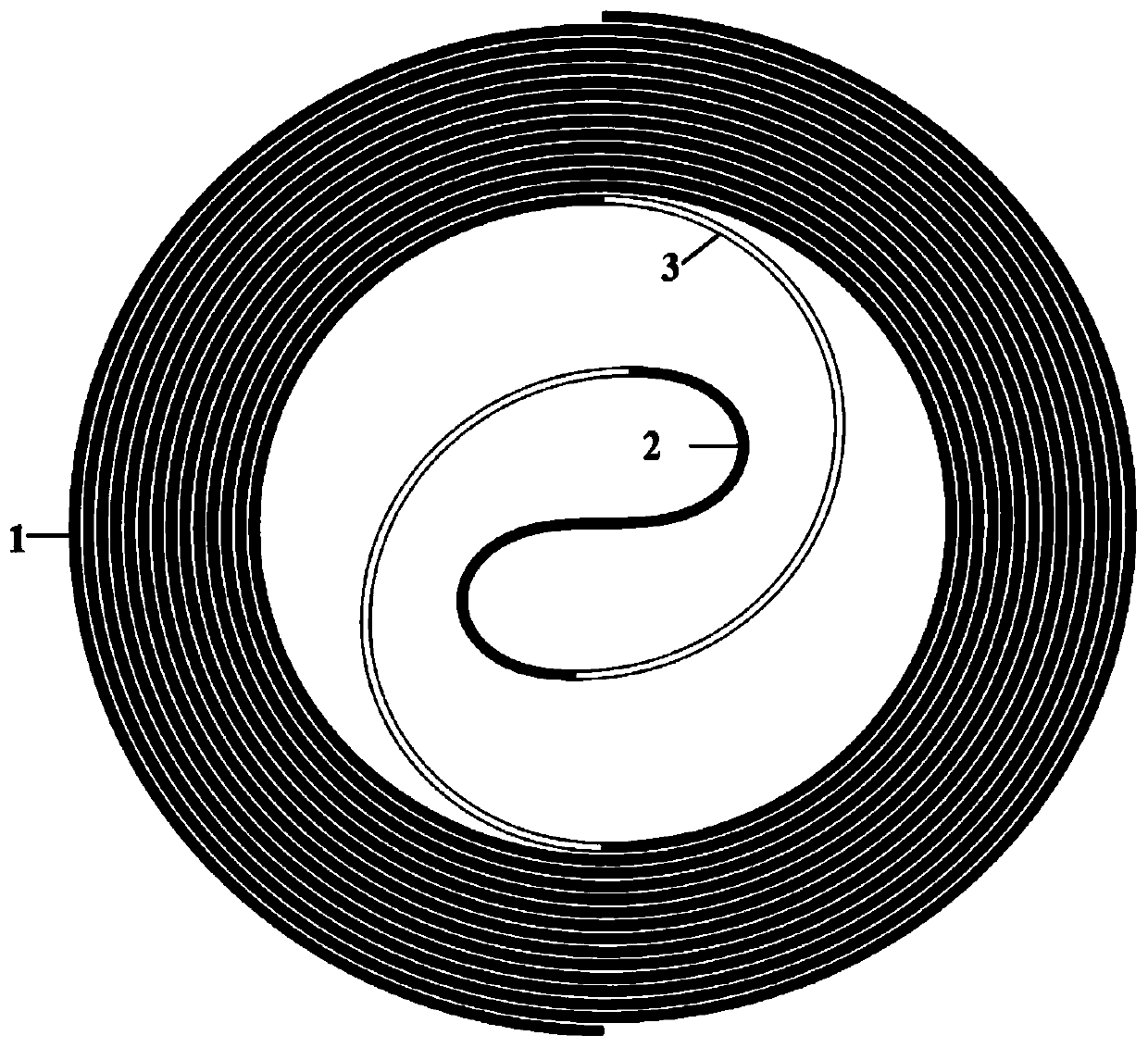
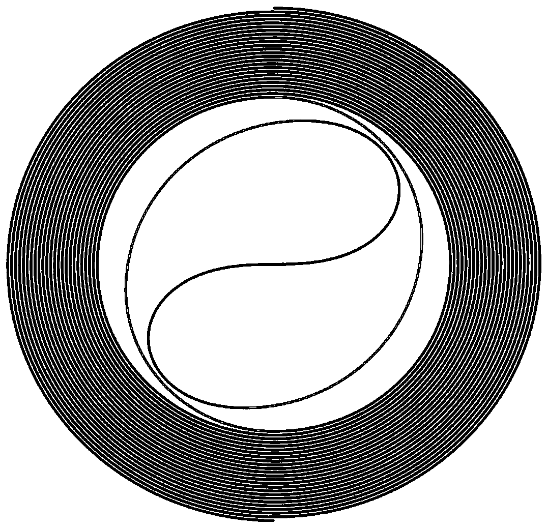
[0029] Such as figure 1 As shown, the specific implementation includes two gradual curvature type spirally curved multimode waveguides 1, one gradual curvature type S-curved multimode waveguide 2 and two curved waveguides 3, the gradual curvature type S-curved multimode waveguide 2 is placed in the curvature gradient type spiral The center of the curved multimode waveguide 1; two gradual curvature type spirally curved multimode waveguides 1 are arranged in a cross-circular spiral inside and outside, and the outer end of one of the gradient curvature type spirally curved multimode waveguides 1 serves as the delay line of the silicon-based multimode spiral waveguide The input end, the inner end is connected via a curved waveguide 3 to one end of the gradually-graded curvature S-bend multimode waveguide 2, and the other end of the gradually-gradual curvature S-bend multimode...


PUM


Abstract

The invention discloses a silicon-based multimode helical waveguide delay line supporting low-loss fundamental mode transmission. A curvature gradual change type S bending multimode waveguide is placed at the centers of curvature gradual change type helical bending multimode waveguides; and two curvature gradual change type helical bending multimode waveguides are annularly and helically arranged,an inner end of one curvature gradual change type helical bending multimode waveguide is connected with one end of the curvature gradual change type S bending multimode waveguide through a bending waveguide, the other end of the curvature gradual change type S bending multimode waveguide is connected with the inner end of the other curvature gradual change type helical bending multimode waveguidethrough another bending waveguide, and the entire silicon-based multimode helical waveguide delay line is arranged in a central symmetry manner. The silicon-based multimode helical waveguide delay line disclosed by the invention can effectively avoid mode mismatch loss and inter-mode crosstalk caused by the abrupt curvature change of the traditional structure, and can reduce the scattering loss introduced by a waveguide sidewall, thereby obtaining low-loss fundamental mode transmission in the silicon-based multimode helical waveguide, and the silicon-based multimode helical waveguide delay line has the advantages of low loss and compact structure and the like, and can be applied to optical buffers, optical delay lines and other systems.

Description

Technical field [0001] The invention relates to a silicon-based multi-mode spiral waveguide delay line supporting low-loss fundamental mode transmission, and more specifically to a silicon-based multi-mode spiral waveguide delay line supporting low-loss fundamental mode transmission. Background technique [0002] With the increasing development of photonic integration technology, many applications for photonic integration, such as: communication network filters and multiplexers, optical gyroscope angular velocity sensors, optical buffers and adjustable true delay lines, etc., all of these systems require light in The on-chip propagation distance is long or a resonant cavity with a high quality factor is required. The realization of the above performance requires that the total transmission loss of the mode in the planar optical waveguide be sufficiently small. [0003] In a planar optical waveguide, the total mode transmission loss is the sum of multiple losses including material ...

Claims


Application Information

Patent Timeline
IPC IPC(8): G02B6/28G02B6/122
CPCG02B6/122G02B6/2861
Inventor 戴道锌王依
Owner ZHEJIANG UNIV
Learn More